Methods of using thin metal layers to make carbon nanotube films, layers, fabrics, ribbons, elements and articles

a carbon nanotube and metal layer technology, applied in the field of carbon nanotube films, layers, fabrics, etc., can solve the problems of difficult control of statistical variance of nanotube wire geometries so grown, high cost, and difficulty in commercial use of modern technology techniques, so as to reduce the rate, increase the resistance of non-woven fabrics, and reduce the density

Active Publication Date: 2009-04-30
ZEON CORP
View PDF99 Cites 55 Cited by
  • Summary
  • Abstract
  • Description
  • Claims
  • Application Information

AI Technical Summary

Benefits of technology

[0031]According to another aspect of the invention, carbon containing gas is applied at a controlled rate and wherein the rate may be decreased to decrease the density and increase the resistance of the non-woven fabric.
[0032]According to another aspect of the invention, the chemical vapor deposition is applied at a controlled temperature and wherein the temperature may be decreased to decrease the density and increase the resistance of the non-woven fabric.
[0033]According to another aspect of the invention, the co-catalyst is applied to a controlled thickness and wherein the controlled thickness may be decreased to decrease the density and increase the resistance of the non-woven fabric.

Problems solved by technology

This form of memory requires highly specialized wire junctions and may not retain non-volatility owing to the inherent instability found in redox processes.
These techniques are now believed to be difficult to employ at commercial scales using modern technology.
Moreover, they may contain inherent limitations such as the length of the nanotubes that may be grown reliably using these techniques, and it may difficult to control the statistical variance of geometries of nanotube wires so grown.
The reliable fabrication of electrically conductive, ultra-thin metallic layers and electrodes in the sub-10 nm regime is problematic.
Metal films in this size regime are usually non-continuous and not conductive over macroscopic distances.
Furthermore, these sub-10 nm films are prone to thermal damage by electrical current, making them unsuitable for applications such as electrical interconnects in semiconductor devices.
Conventional interconnect technologies have a tendency to suffer from thermal damage and metal diffusion eroding the performance of the semiconductor devices especially from degradation of the electrical properties.

Method used


Image

  • Methods of using thin metal layers to make carbon nanotube films, layers, fabrics, ribbons, elements and articles
  • Methods of using thin metal layers to make carbon nanotube films, layers, fabrics, ribbons, elements and articles
  • Methods of using thin metal layers to make carbon nanotube films, layers, fabrics, ribbons, elements and articles

Examples


example 1

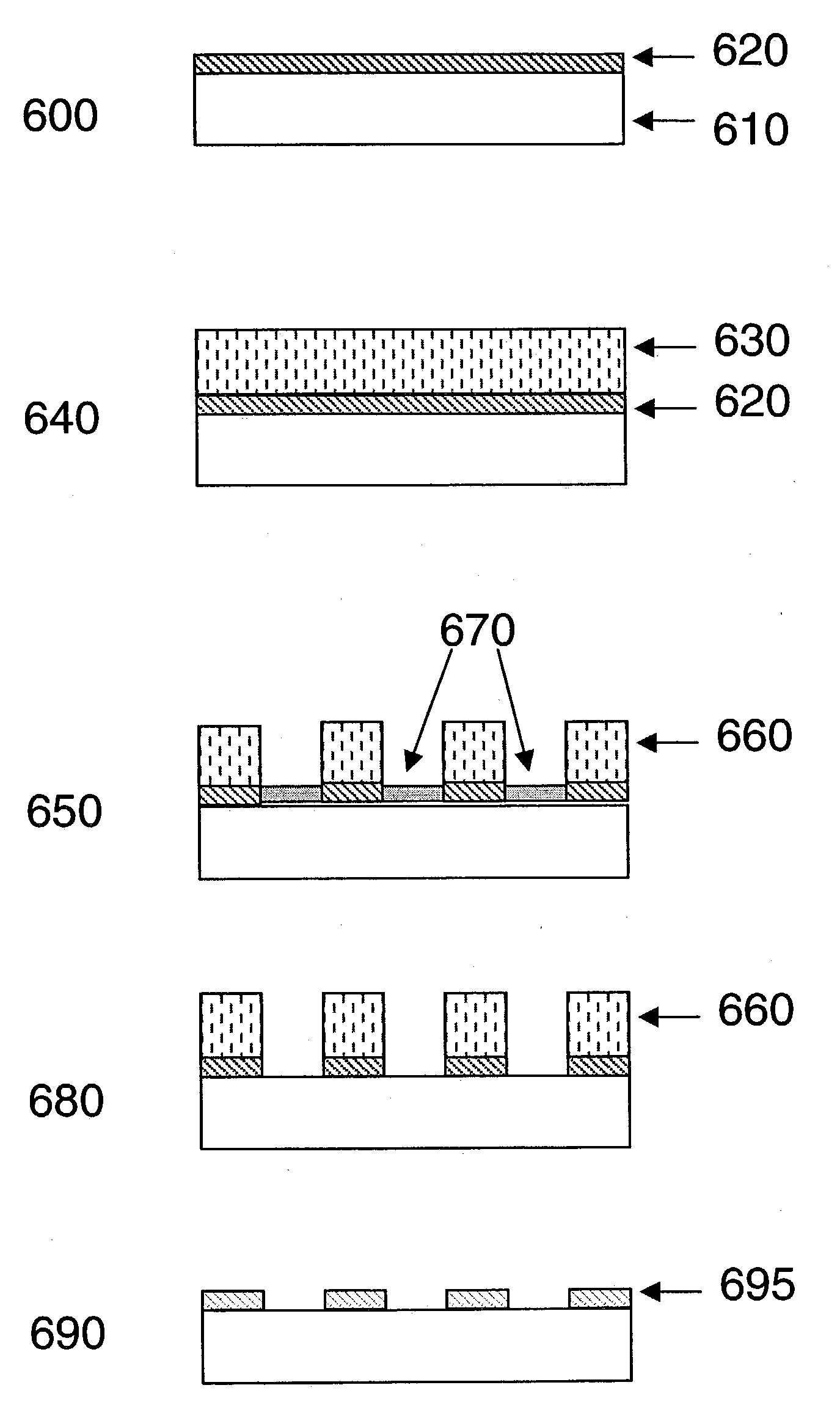
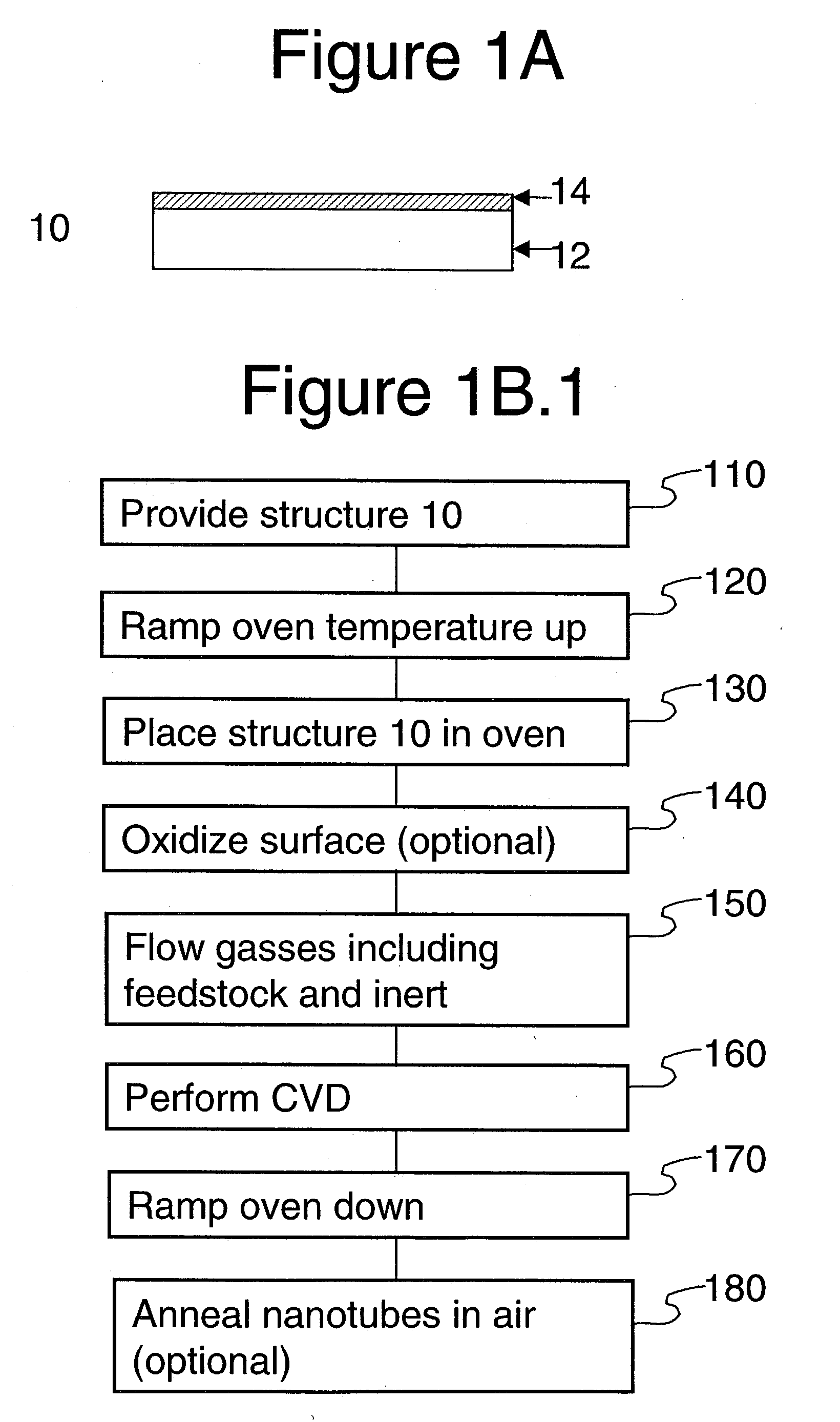
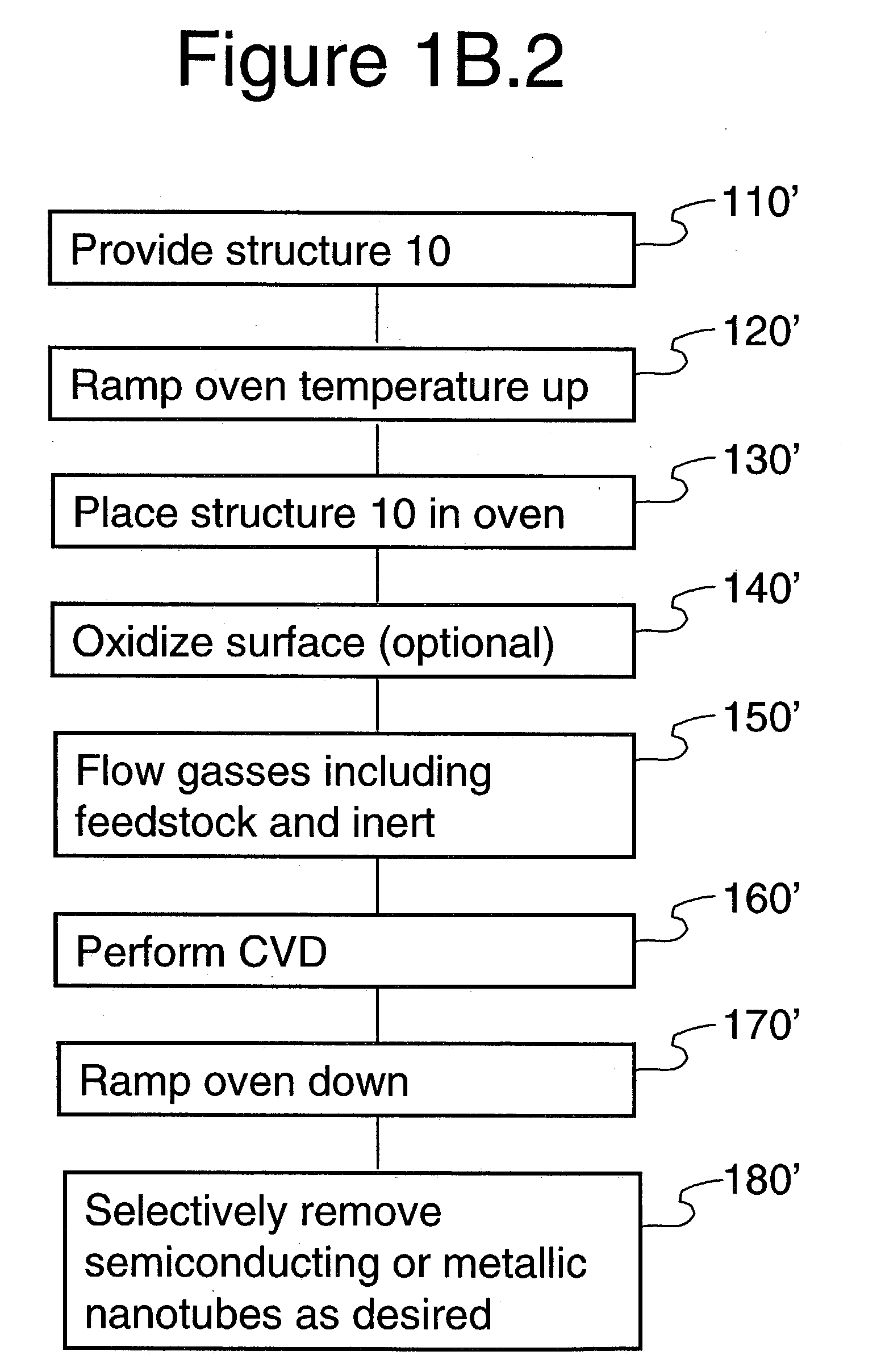
[0082]Thin metal layers of aluminum, iron, and molybdenum (15 nm, 1 nm, and 2 nm, respectively) are sequentially deposited on a substrate. The substrate is placed in a tube furnace in which the temperature is ramped to 500° C. and held for thirty minutes, in an ambience of air. The temperature is then ramped to a CVD temperature of 850° C. in a flow of argon gas and hydrogen gas, at 100:400 sccm Ar:H2 Upon reaching the CVD temperature, methane gas at a flow rate of 500 sccm is introduced into the furnace for a 1 minute growth time. Completing the CVD, the furnace is ramped down to below 200° C. in an argon atmosphere. FIG. 1C is a micrograph of a fabric made from this procedure.

example 2

[0083]All parameters of example 1 are duplicated except in place of methane, ethylene is used at a flow rate of 5.0 sccm for 10 minutes, the CVD temperature is 800° C. The same types of metal layers are employed; however, the thicknesses of the metal layers used are 5 nm aluminum, 1 nm iron, and 2 nm molybdenum. FIG. 1D is a micrograph of the nanotube growth resulting from such use of ethylene.

examples 3-6

[0084]Examples 3-6 show that the rate of methane gas flow affects the production of nanotube fabrics in typical CVD methods. From the micrographs one can see how the change in gas flow from 725 to 500 to 250 sccm affects the amount of growth. These examples show that the porosity and type of nanotubes grown may be controlled by changing specific parameters in the growth process. The growth of nanotubes is sustained over this range and can be finely controlled to generate primarily multilayer fabrics (750 sccm) to primarily monolayer fabrics (250 sccm). Reduction in gas flow to even lower levels is possible to assure primarily monolayer fabrics. An increase of the concentration would allow growth of fabrics with multilayers. Other parameters such as growth time and temperature can be controlled in concert with feedstock gas flow to provide more control over the fabric's characteristics.

[0085]Example 3: Methane is flowed at 725 sccm and the argon and hydrogen gas flow are kept constan...


PUM

PropertyMeasurementUnit
thicknessaaaaaaaaaa
thicknessesaaaaaaaaaa

Abstract

Methods of using thin metal layers to make Carbon Nanotube Films, Layers, Fabrics, Ribbons, Elements and Articles are disclosed. Carbon nanotube growth catalyst is applied on to a surface of a substrate, including one or more thin layers of metal. The substrate is subjected to a chemical vapor deposition of a carbon-containing gas to grow a non-woven fabric of carbon nanotubes. Portions of the non-woven fabric are selectively removed according to a defined pattern to create the article. A non-woven fabric of carbon nanotubes may be made by applying carbon nanotube growth catalyst on to a surface of a wafer substrate to create a dispersed monolayer of catalyst. The substrate is subjected to a chemical vapor deposition of a carbon-containing gas to grow a non-woven fabric of carbon nanotubes in contact and covering the surface of the wafer and in which the fabric is substantially uniform density.

Description

CROSS-REFERENCE TO RELATED APPLICATIONS[0001]This application is related to the following applications, all of which are assigned to the assignee of this application, and all of which are incorporated by reference in their entirety:[0002]Methods of Making Carbon Nanotube Films, Layers, Fabrics, Ribbons, Elements and Articles (U.S. patent application Ser. No. not yet assigned), filed on even date herewith; and[0003]Methods of Using Pre-formed Nanotubes to Make Carbon Nanotube Films, Layers, Fabrics, Ribbons, Elements and Articles (U.S. patent application Ser. No. not yet assigned), filed on even date herewith.[0004]Carbon Nanotube Films, Layers, Fabrics, Ribbons, Elements and Articles (U.S. patent application Ser. No. not yet assigned), filed on even date herewith.BACKGROUND[0005]1. Technical Field[0006]The present invention relates generally to nanotube films, layers, and fabrics and methods of making same and, more specifically to carbon nanotube films, layers, and fabrics and meth...

Claims


Application Information

Patent Timeline
Patent Type & Authority Applications(United States)
IPC IPC(8): H01L21/31
CPCB82Y10/00H01L29/43H01L21/3146Y10S977/742Y10S977/75Y10S977/751H01L21/02115C01B32/16
Inventor WARD, JONATHAN W.RUECKES, THOMASSEGAL, BRENT M.
Owner ZEON CORP
Why Eureka
Try Eureka