CMOS eprom and eeprom devices and programmable CMOS inverters

a technology of cmos and eeprom, which is applied in the direction of semiconductor devices, instruments, electrical apparatuses, etc., can solve the problems of high density of embedded non-volatile memories, high power dissipation of floating-gate nfet memory devices, and only about half the performance of pfet select devices

Active Publication Date: 2009-05-07
MARVELL ASIA PTE LTD
View PDF13 Cites 74 Cited by
  • Summary
  • Abstract
  • Description
  • Claims
  • Application Information

AI Technical Summary

Benefits of technology

[0032]In accordance with this invention, CMOS non-volatile memory devices are provided, including EPROM (Electrically Programmable Read-Only Memory) devices without an erase device, EEPROM (Electrically Erasable And Programmable Read-Only Memory) devices with an erase device, and inverters that are programmable or erasable and programmable. The CMOS non-volatile memory devices of this invention can be built using a standard CMOS logic process, provided that the floating-gate memory FET has negligible gate leakage current. The floating-gate pFET comprises a thick-oxide transistor, which has the advantage that it resists tunneling unwanted discharge therethrough causing loss of data stored in the device.

Problems solved by technology

Often, the additional requirements for such embedded non-volatile memories are high density, i.e. small cell size, low power, and high speed.
A problem with such a device are first that a pFET select device has only about half the performance of a nFET select device and second that a floating-gate nFET used as memory device has much higher power dissipation compared with a floating-gate pFET employed as a memory device.
A problem with such a device is that the resulting memory element, consisting of an nFET and a pFET, is significantly larger than the present invention where only the floating-gate pFET is used as memory element.
A problem with such a device is that a very large area is taken up by the floating-gate memory element which covers all three transistors.
In addition, Brahmbhatt is built using bulk CMOS devices which have an additional problem that the pFET is built using an n-well and the nFETs are built using a p-well.
In Chorr memory elements and logic elements are made on different silicon chips by different process flows, with the problem that the device lacks the desirable attribute of integrating all the desired logic circuits and memory functions on a single chip.
A problem with such an nFET memory device is that it requires more power dissipation to program a floating-gate nFET than a floating-gate pFET.
A problem with such a device is that a pFET access transistor has only about half the performance of an nFET access transistor.

Method used


Image

  • CMOS eprom and eeprom devices and programmable CMOS inverters
  • CMOS eprom and eeprom devices and programmable CMOS inverters
  • CMOS eprom and eeprom devices and programmable CMOS inverters

Examples


first embodiment

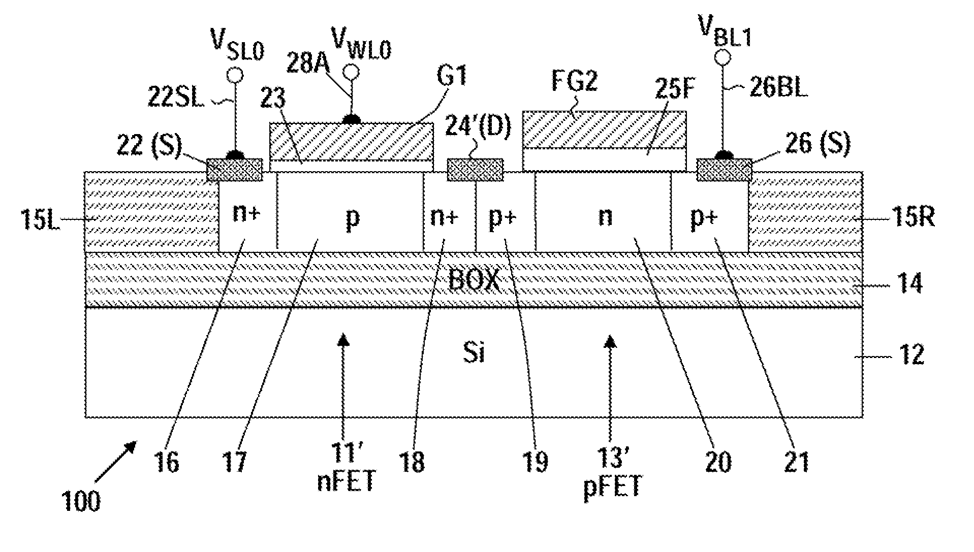
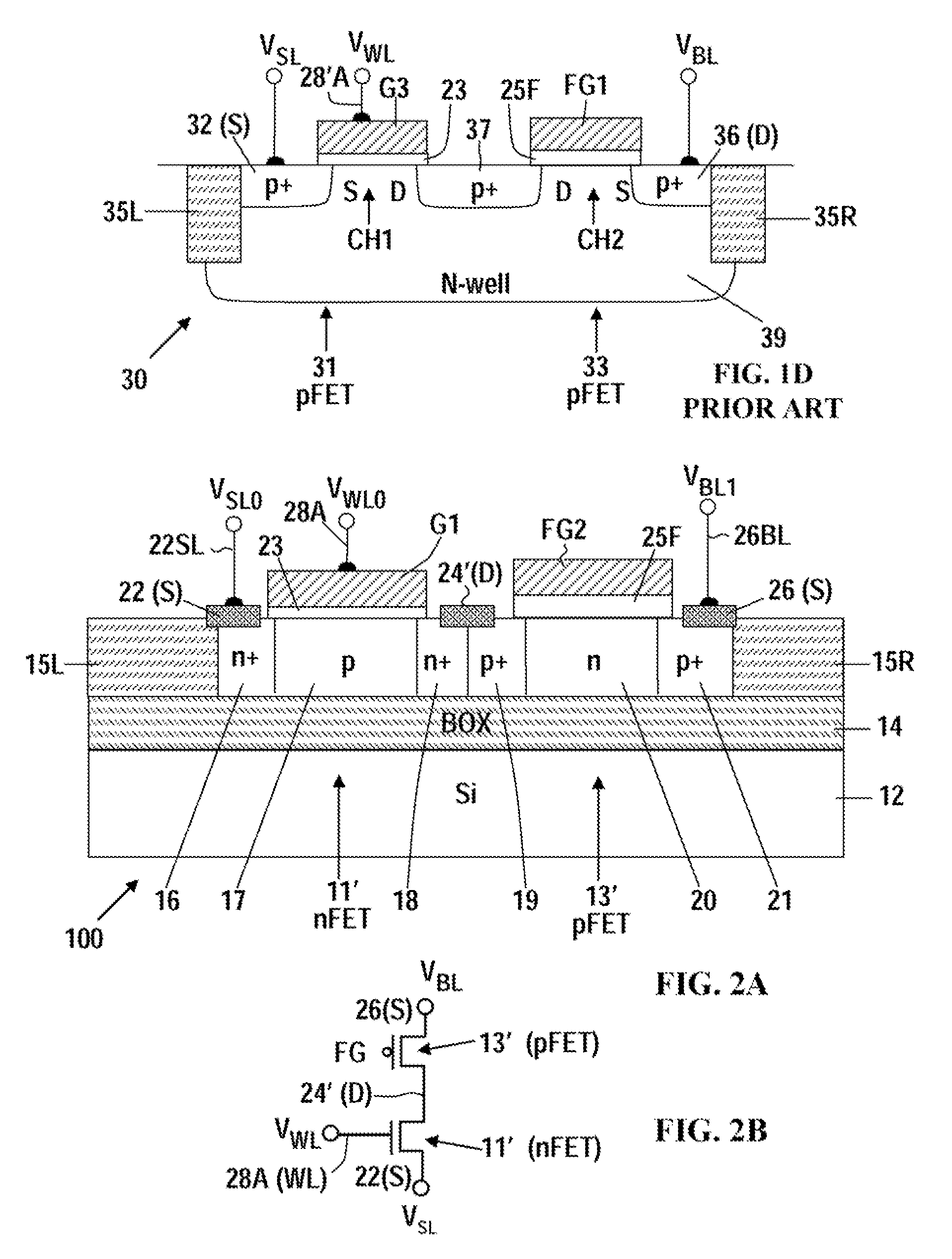
[0072]FIG. 2A is a cross-sectional, schematic view of non-volatile, EPROM cell 100 in accordance with this invention, that is a modification of the inverter 10 of FIG. 1A that includes an access nFET 11′ and a floating gate, storage pFET 13′ formed on a SOI layer on a BOX substrate. The access nFET 11′ includes a gate electrode G1 connected to a WL0 word line 28A and a source contact 22(S) connected to a SL0 select line 22SL. The storage pFET 13′ has a floating gate electrode FG2 and a source contact 26(S) connected to a BL1 bitline 26BL. A common, floating, drain contact 24′(D), that connects drain regions of the access nFET 11′ to the drain region of the floating gate, storage pFET 13′, is not connected to any external line.

[0073]For the CMOS configuration of FIG. 2A, the lowest voltage is applied to the source contact 22(S), which is the source of the access nFET device 11′. Source contact 26(S) will have the highest voltage, which is the source of the pFET device 13′.

[0074]FIG. ...

second embodiment

[0090]FIG. 4A shows an embodiment comprising a CMOS non-volatile EEPROM cell 400A in accordance with this invention, that is a modification of the EPROM cell 100 of FIG. 2A, which includes an erase device 40 and incorporates a third isolation oxide region 15C on the top surface of the BOX layer 14, is located to the right of the p+ doped source region of the storage pFET 13′. The third isolation oxide region 15C is juxtaposed with the erase device 40 which has an erase gate electrode EG that is electrically connected by an electrical conductor line 44 to the floating gate electrode FG2.

[0091]The erase device 40 can be simply one half of an FET with a second thick gate dielectric layer 27 substantially equal in thickness to the thick gate dielectric 25F of the pFET 13′. The erase device 40 includes a p doped region 41P and an n+ doped region 42 formed in the SOI layer on the top surface of the BOX layer 14. The p doped region 41P is juxtaposed with the right edge of the third isolati...

third embodiment

[0095]FIG. 4C shows a CMOS non-volatile EEPROM cell 400B in accordance with this invention, which is a modification of the EEPROM cell 400A of FIG. 4A. In FIG. 4C, the p-doped region 41P of FIG. 4A, under the erase gate electrode EG, has been replaced by an n-doped region 41N to increase the overlap of the erase gate EG with the n-type region 41N and n+ doped region 42.


PUM


Abstract

A CMOS EPROM, EEPROM or inverter device includes an nFET device with a thin gate dielectric layer and a pFET device juxtaposed with the nFET device with a thick gate dielectric layer and a floating gate electrode. The thick gate dielectric layer is substantially thicker than the thin gate dielectric layer. A common drain node connected both FET devices has no external connection in the case of a memory device and has an external connection in the case of an inverter. There are external circuit connections to the source regions of both FET devices and to the gate electrode of the nFET device. The pFET and nFET devices can be planar, vertical or FinFET devices.

Description

BACKGROUND[0001]This invention relates to Complementary Metal Oxide Silicon (CMOS) Electrically Programmable Read Only Memory (EPROM) and CMOS EEPROM (Electrically Erasable and Programmable Read Only Memory) devices, which are especially suitable for embedded applications.[0002]In many applications, particularly in System-on-Chip (SoC) applications, designers want to have a certain number of embedded non-volatile memory devices on the microprocessor or Application-Specific Integrated Circuit (ASIC) chips. The preferred approach for meeting this need is to provide embedded non-volatile memories that require little or no additional process cost to the base logic technology. Often, the additional requirements for such embedded non-volatile memories are high density, i.e. small cell size, low power, and high speed.[0003]In a regular CMOS logic process, non-volatile memory devices are typically made using charge storage in a floating gate electrode. In general, it takes a lower voltage t...

Claims


Application Information

Patent Timeline
Patent Type & Authority Applications(United States)
IPC IPC(8): H01L27/092H01L27/12
CPCG11C16/0433G11C16/10H01L21/823857H01L21/823885H01L21/84H01L27/0922H01L29/7881H01L27/11521H01L27/11524H01L27/11558H01L27/1203H01L29/66825H01L29/785H01L27/105H10B41/30H10B41/60H10B41/35
Inventor CAI, JINNING, TAK H.SAFRAN, JOHN M.
Owner MARVELL ASIA PTE LTD
Why Eureka
Try Eureka