Transient voltage suppressor manufactured in silicon on oxide (SOI) layer

a technology of transient voltage suppressor and silicon oxide, which is applied in the direction of semiconductor devices, diodes, electrical apparatus, etc., can solve the problems of sudden and strong voltage snapback, system instability or even damage, and the conventional technology of designing and manufacturing transient voltage suppressors are still confronted with certain technical difficulties, so as to prevent latching and reduce parasitic capacitance

Inactive Publication Date: 2009-05-07
ALPHA & OMEGA SEMICON LTD
View PDF13 Cites 46 Cited by
  • Summary
  • Abstract
  • Description
  • Claims
  • Application Information

AI Technical Summary

Benefits of technology

[0009]It is therefore an aspect of the present invention to provide a new and improved device structure to implement a TVS in the SOI structure to reduce the parasitic capacitance and to prevent the latch-up of the parasitic PNP-NPN transistors such that the above-discussed difficulties and limitations encountered by the conventional TVS array can be overcome.
[0010]Another aspect of the present invention is to form the TVS protective circuit in the SOI layer. The lateral distance between adjacent diodes can be reduced without the concerns of parasitic capacitance and inadvertent latch-up.

Problems solved by technology

The conventional technologies for designing and manufacturing transient voltage suppressor (TVS) are still confronted with certain technical difficulty.
The latch-up may cause sudden and strong voltage snapback.
The sudden and large snapback may cause the undesired effects of system instability or even damages.
Additionally, the latch-up of the parasitic NPN or PNP transistors in the TVS array may further lead to other unexpected or undesirable voltage-current transient conditions.
The technical difficulties caused by the parasitic capacitance and parasitic PNP or NPN latch-up in a device implemented with the TVS protection cannot be easily resolved.
However, in situations such as electrostatic discharge (ESD), electrical fast transients and lightning, an unexpected and uncontrollable high voltage may accidentally strike onto the circuit.
However, the PN junction type of TVS has no minority carriers and has a poor clamping performance due to its high resistance as that shown in FIG. 1B.
Additionally, as shown in FIG. 2C, such implementation further generates another problem of latch-up due to the silicon-controlled rectifier (SCR) action induced by parasitic PNP and NPN transistors.
The main Zener diode breakdown triggers the NPN on, which further turns on the SCR, resulting in latch-up.
To suppress latch-up due to the SCR action induced by parasitic PNP and NPN transistors, the actual device implementation on a semiconductor substrate requires a lateral extension on the substrate of a distance that may be up to 100 micrometers or more as shown in FIG. 2B and the suppression usually is not effective enough.

Method used


Image

  • Transient voltage suppressor manufactured in silicon on oxide (SOI) layer
  • Transient voltage suppressor manufactured in silicon on oxide (SOI) layer
  • Transient voltage suppressor manufactured in silicon on oxide (SOI) layer

Examples


Embodiment Construction

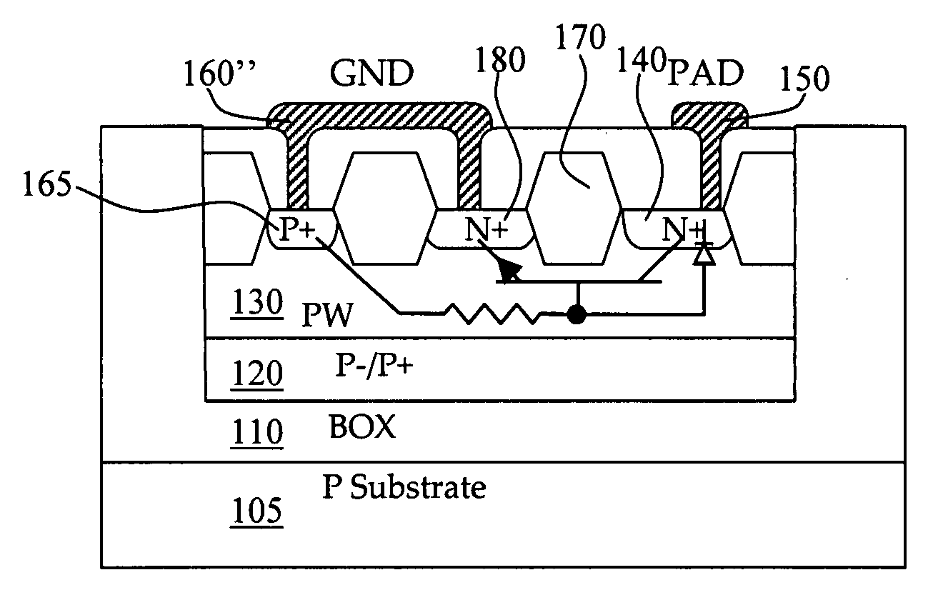
[0024]FIGS. 3A to 3C are a cross sectional views showing the clamp diode and the high / low side diode of the TVS formed on a silicon on insulator (SOI) of this invention. A thick body oxide (BOX) layer 110 is deposited on a P type substrate 105. The BOX layer 110 has a thickness in the range of 250 A to 1 um to sustain an application with a breakdown voltage higher than 25 volts. Formation of BOX may be carried out by forming a thick oxide layer on top surface of P− wafers then bonding and fusing the oxide layers of two wafers face to face together then lapping the substrate to a desired thickness, which is a well known process. Optional deep dopant implant may be applied to convert a P− substrate layer above the BOX layer into a P+ layer. In the embodiment as shown in FIG. 3A, the clamp diode is formed in a P well (PW) 130 on top of an optional P− / P+ substrate layer 120. A grade doping profile of P doped region 135 provides trigger voltage adjustment for a clamp diode formed by the ...


PUM


Abstract

A transient voltage-suppressing (TVS) device supported on a semiconductor substrate is applied to protect an electronic device from a transient voltage. The TVS device includes a clamp diode functions with a high-side and a low side diodes for clamping a transient voltage disposed on a top layer of the semiconductor substrate insulated by a insulation layer constituting a TVS on silicon-on-insulator (SOI) device. In an exemplary embodiment, the insulator layer further includes a thick body oxide (BOX) layer having a thickness in the range of 250 Angstroms to 1 micrometer to sustain an application with a breakdown voltage higher than 25 volts. In another exemplary embodiment, the clamp diode further surrounded by a P-well and the P-well is formed on top of a P− / P+ substrate layer disposed above the insulator layer.

Description

BACKGROUND OF THE INVENTION[0001]1. Field of the Invention[0002]The invention relates generally to a circuit configuration and method of manufacturing a transient voltage suppressor (TVS). More particularly, this invention relates to an improved circuit configuration and method of manufacturing TVS in a silicon-on-insulator (SOI) layer for providing TVS protection with low capacitance.[0003]2. Description of the Relevant Art[0004]The conventional technologies for designing and manufacturing transient voltage suppressor (TVS) are still confronted with certain technical difficulty. Particularly, when the TVS is formed with multiple PN junctions diodes in a semiconductor substrate by applying standard CMOS processing steps, there are inherent PNP and NPN parasitic transistors. In an ESD event or the occurrence of a transient voltage, with a larger voltage applied to this TVS array, the parasitic NPN or PNP transistors are turned on and latched up. The latch-up may cause sudden and stro...

Claims


Application Information

Patent Timeline
Patent Type & Authority Applications(United States)
IPC IPC(8): H01L27/06H01L21/8222
CPCH01L21/84H01L27/1203H01L27/0255H01L29/861H01L29/866H01L29/0649
Inventor MALLIKARJUNASWAMY, SHEKAR
Owner ALPHA & OMEGA SEMICON LTD
Why Eureka
Try Eureka