Methods for improving image quality of image detectors, and systems therefor

a detector and image technology, applied in image enhancement, instruments, therapy, etc., can solve the problems of small bias voltage of the sensor for proper operation, errors in the calculated intensity of the associated image pixel, and other imaging devices that convert radiation to electrical charge suffer from similar dark current problems, so as to improve long-term stability and eliminate line artifacts

Inactive Publication Date: 2009-05-21
DEUTMANN HEINZ
View PDF15 Cites 35 Cited by
  • Summary
  • Abstract
  • Description
  • Claims
  • Application Information

AI Technical Summary

Benefits of technology

[0012]The imaging device is preferably an amorphous silicon flat panel with sensors deployed in a two-dimensional array. The XRD 1640 series, offered by PerkinElmer®, Inc. of Fremont, Calif., is one suitable device series. The sensors of the imaging device record the intensity of received light as stored electrical charge, and may be read to capture an image frame. The captured image frames are then corrected to create an image of the radiation field, thereby allowing quick and efficient verification of the treatment field including patient anatomy, patient position and beam shape.
[0020]Accordingly, the second aspect of the invention provides a method of gain separation of an imaging device, comprising the iterative steps of: (a) providing an nth order estimation of the dose profile image of the beam irradiated onto the imaging device (which can be uniform in a 0th order first guess); (b) subtracting from the uncorrected flood field image the clean offset image; (c) dividing the result of the subtraction by the estimated dose profile image of the beam to derive a pixel sensitivity image; (d) multiplying the result of the division with the doserate of the beam at a central pixel of the imaging device to renormalize; (e) adding the corrected offset image to obtain a gain image with the influence of an inhomogeneous flood field eliminated; (f) separating this flat image according to the steps in the first part of the invention to eliminate line artifacts; (g) multiply with the estimated dose profile image of nth order; and (h) low pass filter this image to derive a (n+1)th order estimation of the dose profile image of the beam irradiated onto the imaging device. Steps (b) to (h) can be repeated until the estimation of the dose profile is converging to a stable value, typically less then 5 iterations are needed. No further iteration is required to calculate the pixel sensitivity image of a panel if a dose profile is provided from separate image analysis or independent measurements in advance.
[0022]Therefore, a further aspect of the present invention relates to dynamic offset correction using a background image. The background image acquired with an imaging device such as an amorphous silicon panel describes the dark field, i.e. the panel signal without any radiation. The background image is significantly varying with temperature and age of a panel. Therefore, according to this aspect of the invention a method is provided to acquire a dark field image immediately before the radiation is turned on and correct the clinical image for changes in the offset. Currently available medical flat panel software does already consider dynamic background measurements. As a new aspect according to the invention, the acquired offset image is separated from ghost contributions and moreover used to modify the doserate vs. pixel signal curve, i.e. the gain images of the panel. The modified curve is then used for image correction. This dynamic offset measurement is advantageous in that it can be done automatically between treating patients during the day, and no additional calibration work of engineers or physicists has to be done, which is highly important in clinical environments.
[0026]The method of this aspect is preferably performed when the time elapsed since the last image was captured, i.e. the panel was irradiated, exceeds a preset threshold to ensure that any lag (ghost) information of previously irradiated beams has vanished. The threshold is for example 5 minutes. Preferably, a second time threshold is taken into account, i.e. the time lapsed since the last valid background measurement was performed. Such threshold is larger than the first threshold and for example 7 minutes, and guarantees that an imaging device will not just be busy with capturing background images.

Problems solved by technology

However, the photodiodes of the amorphous silicon sensors require a small bias voltage for proper operation.
This dark current thereby causes errors in the calculated intensity of the associated image pixel.
Other imaging devices that convert radiation to electrical charge suffer from similar dark current problems.
Since the device is irradiated with high energy photon beams, scattered dose (and occasionally the primary beam) damages the electronic components of the readout system (amplifiers) of the panel, so that the average life span of a clinically useable panel under such conditions may often not exceed 18 months.
However, offset correction, gain correction or recalibration often fails to provide suitable improvements with respect to image quality and life span of aged panels.

Method used


Image

  • Methods for improving image quality of image detectors, and systems therefor
  • Methods for improving image quality of image detectors, and systems therefor
  • Methods for improving image quality of image detectors, and systems therefor

Examples


Embodiment Construction

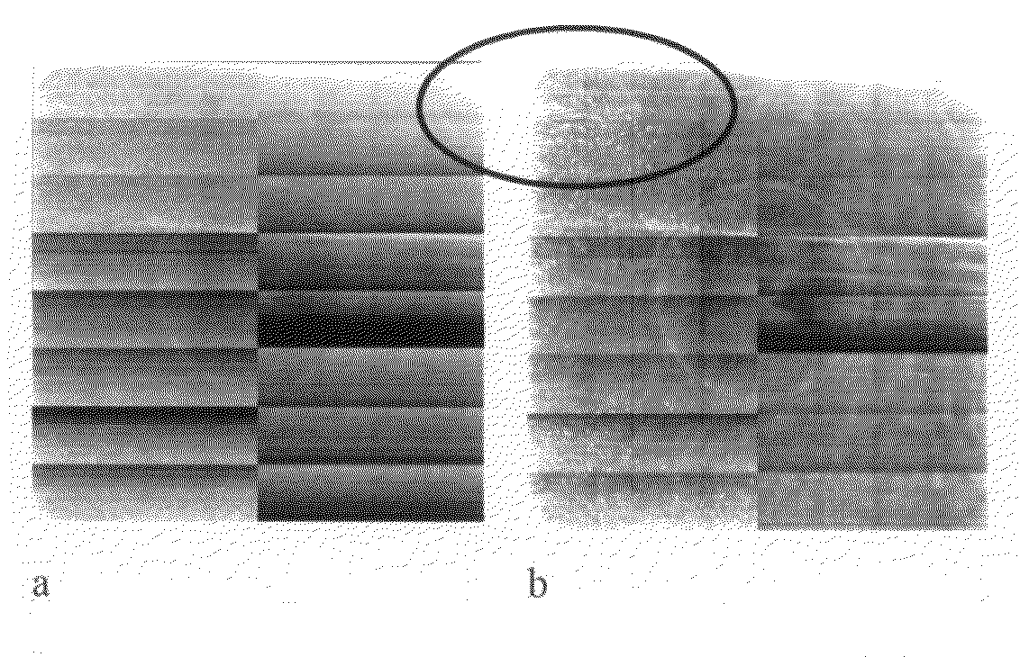
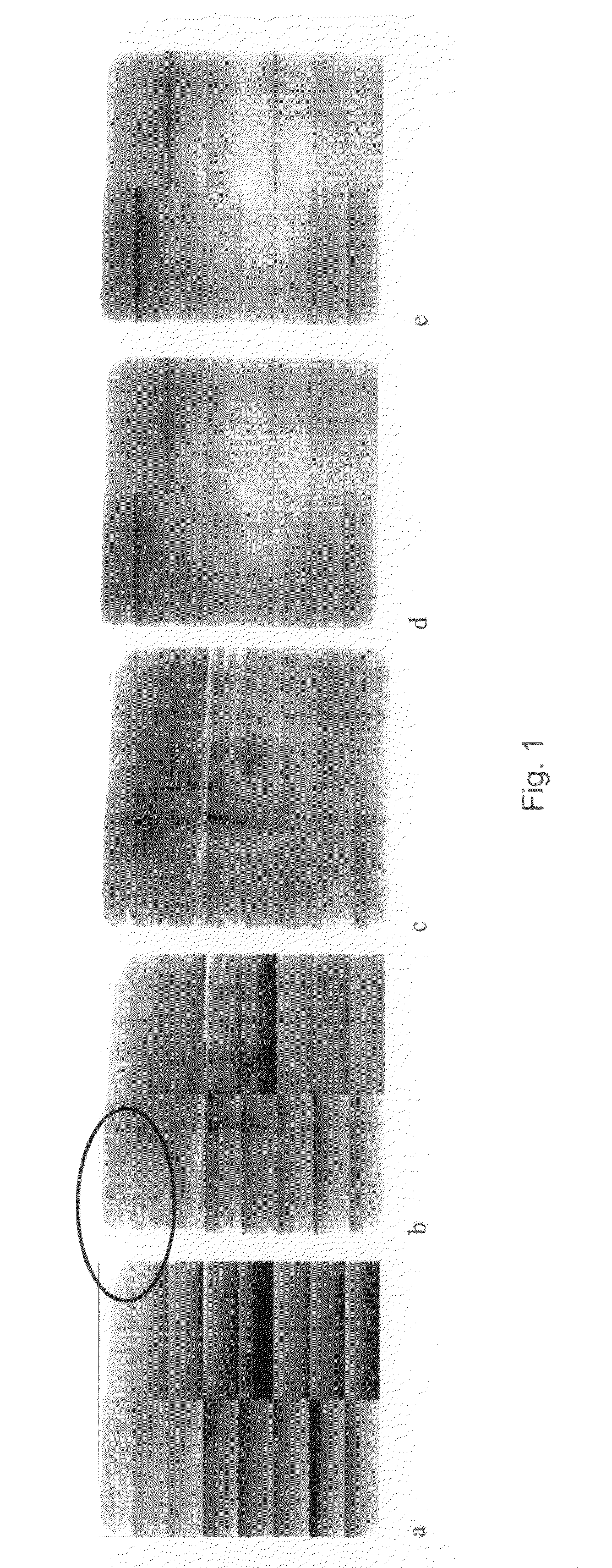
[0066]Background images of older panels show disturbing horizontal lines parallel to the long sides of the panel. This is shown, as an example, in FIG. 1. FIG. 1 shows uncorrected images of an old panel at different doserates. As can be seen, the dark offset stripes are rapidly disappearing with increasing doserate which is in FIG. 1a 7 MU / min, FIG. 1b 25 MU / min, FIG. 1c 50 MU / min, FIG. 1d 100 MU / min and FIG. 1e 400 MU / min. These high intensity (dark) rows in the offset image vanish rapidly on irradiation with very low doserates (FIGS. 1a-c), and on increasing doserates the stripes turn continuously lighter, indicating that the relative pixel sensitivity for the pixels in such poor rows is significantly decreasing at very low doserates to values comparable to better pixels in other rows.

[0067]The remaining stripes in the images acquired at higher doserates—deviations in the response of different rows in different sub panels—are not necessarily located in the same rows as seen in the...


PUM


Abstract

The present invention relates to methods and systems for improving image quality of imaging devices such as image detectors, and preferably of flat panel detectors such as amorphous silicon flat panel detectors, for example used in radiotherapy. The invention also relates to the improving of life span of used or aged detectors.

Description

TECHNICAL FIELD[0001]The present invention relates to methods and systems for improving image quality of imaging devices such as flat panel detectors like amorphous silicon (aSi:H) flat panels, for example used in radiotherapy. The invention also relates to the improving of life span of used or aged detectors.BACKGROUND OF THE INVENTION[0002]Many types of digital imaging devices create image data using stored electrical charge. For example, known charge-coupled devices (CCDs) convert light to electrical charge and store the electrical charge for subsequent readout. In the case of amorphous silicon devices, a scintillating layer receives X-rays and generates light in proportion to the intensity of the received X-rays. An array of amorphous silicon photodiodes then converts and stores the generated light as electrical charge. For example, a photodiode of an amorphous silicon flat panel accumulates charge in proportion to an intensity of light received from an associated radiation sour...

Claims


Application Information

Patent Timeline
Patent Type & Authority Applications(United States)
IPC IPC(8): G06K9/00G01D18/00G06K9/40H04N5/361H04N5/365
CPCA61N5/1048A61N2005/1054G06T2207/10116A61B6/583H04N5/361H04N5/3651H04N5/3655H04N5/32H04N25/673H04N25/671H04N25/63
Inventor DEUTSCHMANN, HEINZ
Owner DEUTMANN HEINZ
Why Eureka
Try Eureka