Solar cell and manufacturing method thereof

a technology of solar cells and manufacturing methods, applied in the field of solar cells, can solve the problems of increasing manufacturing time and costs, reducing light absorption efficiency of solar cells, and increasing manufacturing costs, and achieve the effect of reducing the thickness of the semiconductor layer and light absorption efficiency

Inactive Publication Date: 2009-06-04
DELTA ELECTRONICS INC +1
View PDF0 Cites 33 Cited by
  • Summary
  • Abstract
  • Description
  • Claims
  • Application Information

AI Technical Summary

Benefits of technology

[0010]The invention provides a solar cell and method for fabricating the same. The invention reduces semiconductor layer thickness, while keeping light absorption efficiency and completeness.
[0013]The invention of a solar cell and method for fabricating the same is based on the conventional silicon thin-film solar cell. The micro- or nano-roughing structure is inserted into the semiconductor layer (such as silicon film) and the upper electrode (such as Transparent Conductive Oxide, TCO) to increase the optical path, raising the absorption efficiency of the silicon thin-film and reduce the minimal thickness of the silicon thin-film so as to improve the efficient usage of the amorphous silicon material, reduce the light degradation of amorphous silicon material and decrease manufacturing time of the micro-silicon material, thus decreasing material and manufacturing costs.

Problems solved by technology

However, in recent years, due to lack of silicon raw materials, thin-film solar cells which do not use silicon raw materials or reduce the quantity thereof, have been developed.
However, after the amorphous silicon material is irradiated by sunlight for a long period of time (called like the light deterioration phenomenon), the interior of the amorphous silicon material will become defective and result in decreased light absorption efficiency of the solar cells.
Thus, increasing manufacturing time and costs.
However, if the thickness of the film is lower than the minimal thickness for efficient sunlight absorption, the absorption coefficient of sunlight may become deficient and result in decreased absorption efficiency.

Method used


Image

  • Solar cell and manufacturing method thereof
  • Solar cell and manufacturing method thereof
  • Solar cell and manufacturing method thereof

Examples


Embodiment Construction

[0024]The following description is of the best-contemplated mode of carrying out the invention. This description is made for the purpose of illustrating the general principles of the invention and should not be taken in a limiting sense. The scope of the invention is best determined by reference to the appended claims.

[0025]The following description is of a solar cell and a manufacturing method thereof and is the best-contemplated mode of the invention.

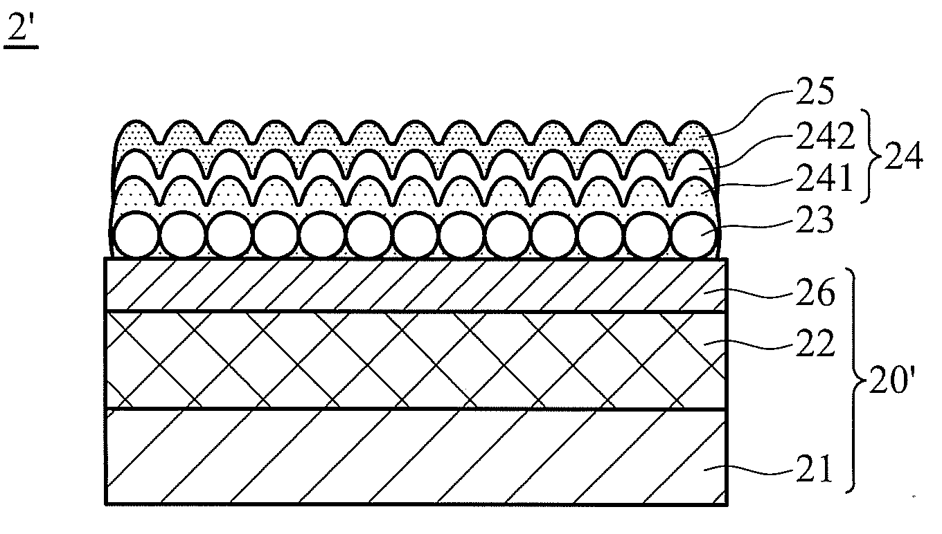
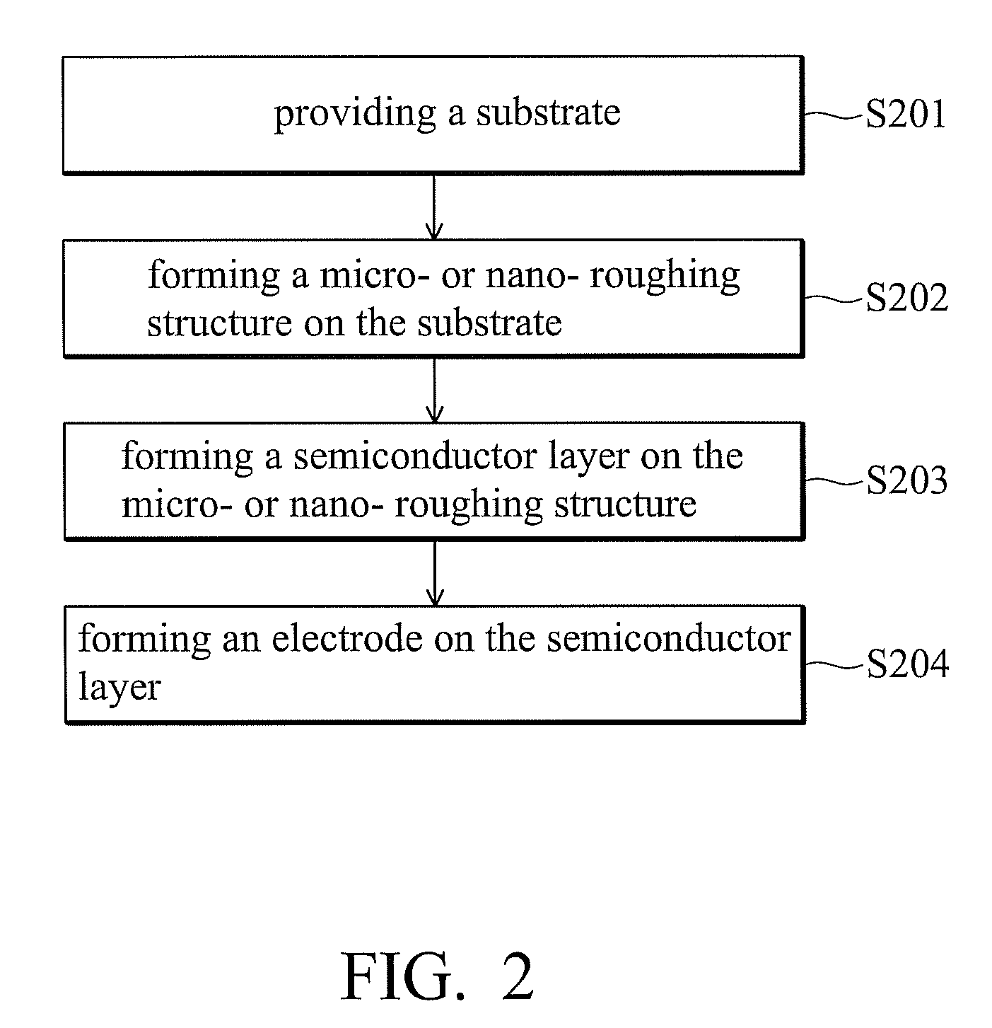
[0026]FIG. 2 is a flow chart of an exemplary embodiment of a method for fabricating a solar cell. FIGS. 3A to 3D show cross sections of each process step according to FIG. 2.

[0027]First, referring to FIG. 3A, a substrate 20 is provided, which is a transparent substrate 21 with a first transparent conductive layer 22 (step S201). The transparent substrate 21 may be, but is not limited to a glass substrate. The first transparent conductive layer 22 may be, but is not limited to a transparent conductive oxide (TCO), such as indium tin ox...


PUM


Abstract

A solar cell and a manufacturing method thereof are provided herein. The solar cell includes a substrate with a first transparent conductive layer, a micro- or nano-roughing structure formed on the first transparent conductive layer, and a semiconductor active layer formed on the micro- or nano-roughing structure and covering the micro- or nano-roughing structure.

Description

CROSS REFERENCE TO RELATED APPLICATIONS[0001]This Application claims priority of Taiwan Patent Application No. 096145567, filed on Nov. 30, 2007, the entirety of which is incorporated by reference herein.BACKGROUND OF THE INVENTION[0002]1. Field of the Invention[0003]The present invention relates to a solar cell and method for fabricating the same, and in particular relates to a solar cell having a micro- or nano-roughing structure in between the substrate and the semiconductor layer so as to increase photo-electricity transformation of the solar cell.[0004]2. Description of the Related Art[0005]Currently, about 90 percent of solar cells are produced from silicon wafers. However, in recent years, due to lack of silicon raw materials, thin-film solar cells which do not use silicon raw materials or reduce the quantity thereof, have been developed. Nevertheless, currently, silicon-based solar cells are mainly produced. As for thin-film solar cells, tandem cells are mainly being develop...

Claims


Application Information

Patent Timeline
Patent Type & Authority Applications(United States)
IPC IPC(8): H01L31/0376H01L31/18
CPCH01L31/02168Y02E10/548H01L31/075H01L31/0236H01L31/02366H01L31/02363
Inventor CHEN, CHII-CHANGCHAN, CHIA-HUAWU, HUANG-NANYAO, FU-YUANCHEN, SHENG-HUISHIEH, HUNG-CHIENLEE, CHENG-CHUNGSHING, TAI-KANG
Owner DELTA ELECTRONICS INC
Why Eureka
Try Eureka