Nonvolatile semiconductor memory device and method of fabricating the same

a semiconductor memory and non-volatile technology, applied in the direction of semiconductor devices, basic electric elements, electrical appliances, etc., can solve the problems of reducing the writing/erasing speed, the insulating film provided between the control electrode is not sufficiently researched, and the element is not suitable for use. , to achieve the effect of higher relative permittivity and higher relative permittivity

Active Publication Date: 2009-06-18
KIOXIA CORP
View PDF15 Cites 45 Cited by
  • Summary
  • Abstract
  • Description
  • Claims
  • Application Information

AI Technical Summary

Benefits of technology

[0009]According to one aspect of the present invention, there is provided a nonvolatile semiconductor memory device comprising a semiconductor substrate, a first insulation layer formed on the semiconductor substrate, a charge storage layer formed on the first insulation layer, a second insulation layer formed on the charge storage layer, a control electrode formed on the second insulation layer, wherein the second insulation layer includes a first silicon oxide film, an intermediate insulating film formed on the first silicon oxide film and having a relative permittivity of not less than 7, and a second silicon oxide film formed on the intermediate insulating film; and a charge trap layer is formed at least in either first or second silicon oxide film or a boundary between the first silicon oxide film and the intermediate insulating film or a boundary between the second silicon oxide film and the intermediate insulating film.
[0010]In one embodiment, the nonvolatile semiconductor memory device further comprises a third insulation layer, instead of the second insulation layer, said third insulation layer including a silicon oxide film, a nitride-containing film formed on the silicon oxide film and a metal oxide film formed on the nitride-containing film and having a relative permittivity of not less than 7.
[0011]In another embodiment, the nonvolatile semiconductor memory device further comprises a fourth insulation layer provided between the charge storage layer and the control electrode, instead of the second insulation layer, said fourth insulation layer including a layer structure of a silicon oxide film, a first high dielectric insulating film which has a higher relative permittivity than a silicon nitride film and a second high dielectric insulating film which has a higher relative permittivity than a silicon nitride film, the first and second high dielectric insulating films being structured so as to interpose the silicon oxide film.
[0012]According to another aspect of the invention, there is provided a method of fabricating a nonvolatile semiconductor memory device, comprising forming a first insulation layer on a semiconductor substrate, forming a charge storage layer on the first insulation layer, forming a second insulation layer on the charge storage layer, and forming a control electrode on the second gate insulating film, wherein the step of forming the second insulation layer includes forming a first silicon nitride film on the charge storage layer, forming a first silicon oxide film on the first silicon nitride film, forming an intermediate insulating film on the first silicon oxide film, the intermediate insulating film having a higher relative permittivity than a silicon nitride film, forming a second silicon oxide film on the intermediate insulating film, and forming a second silicon nitride film on the second silicon oxide film, and in the first and / or second silicon oxide film forming step, the first and / or second silicon oxide film is formed so as to have a charge trap layer.
[0013]According to further another aspect of the invention, there is provided a method of fabricating a nonvolatile semiconductor memory device, comprising forming a first insulation layer on a semiconductor substrate, forming a charge storage layer on the first insulation layer, forming a second insulation layer on the charge storage layer, and forming a control electrode on the second insulation layer, wherein in the second insulation layer forming step, a first silicon oxide film added with nitride is formed on the charge storage layer, an intermediate insulating film is formed on the first silicon oxide film, the intermediate insulating film having a relative permittivity of not less than 7, and a second silicon oxide film is formed on the intermediate insulating film, the silicon oxide film being formed by an atomic layer deposition (ALD) method.

Problems solved by technology

An increase in the interference between the adjacent cells results in malfunction of elements and a reduction in a writing / erasing speed.
However, sufficient research has not conventionally been made about the insulating film provided between the control electrode and the charge storage layer.

Method used


Image

  • Nonvolatile semiconductor memory device and method of fabricating the same
  • Nonvolatile semiconductor memory device and method of fabricating the same
  • Nonvolatile semiconductor memory device and method of fabricating the same

Examples


first embodiment

[0053]the present invention will be described with reference to FIGS. 1 to 14. In the following description, identical or similar parts are labeled by the same reference numerals throughout the embodiments. The drawings typically illustrate the invention, and the relationship between a thickness and plane dimension, layer thickness ratio and the like differ from natural size.

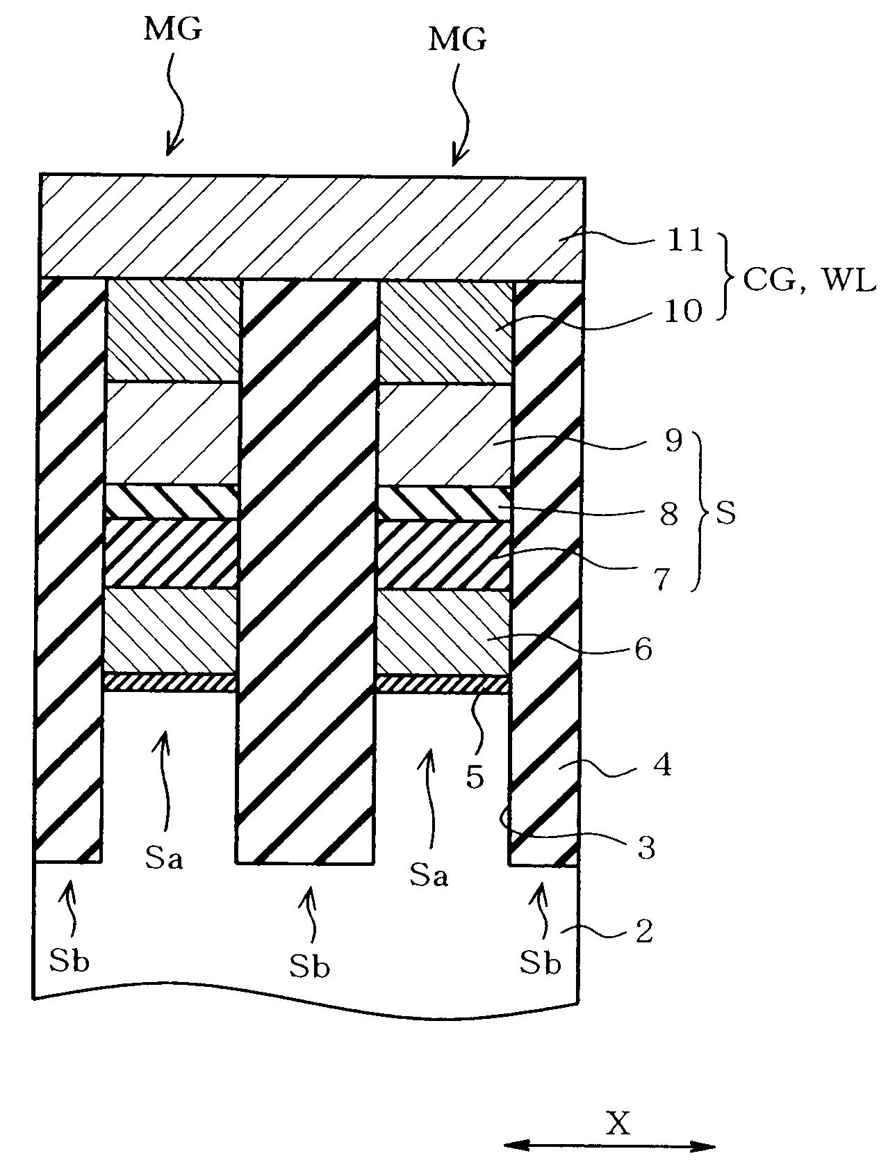
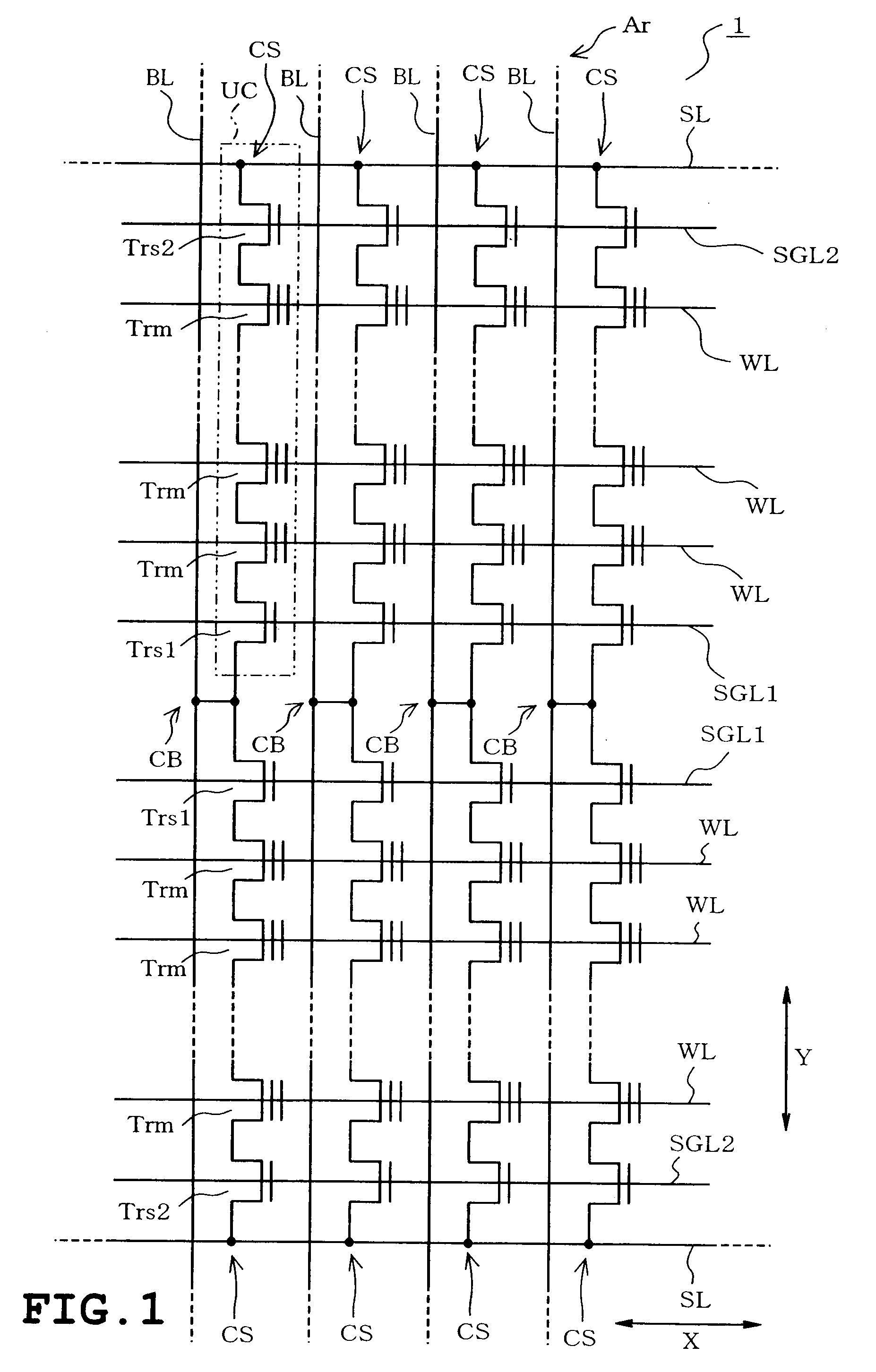
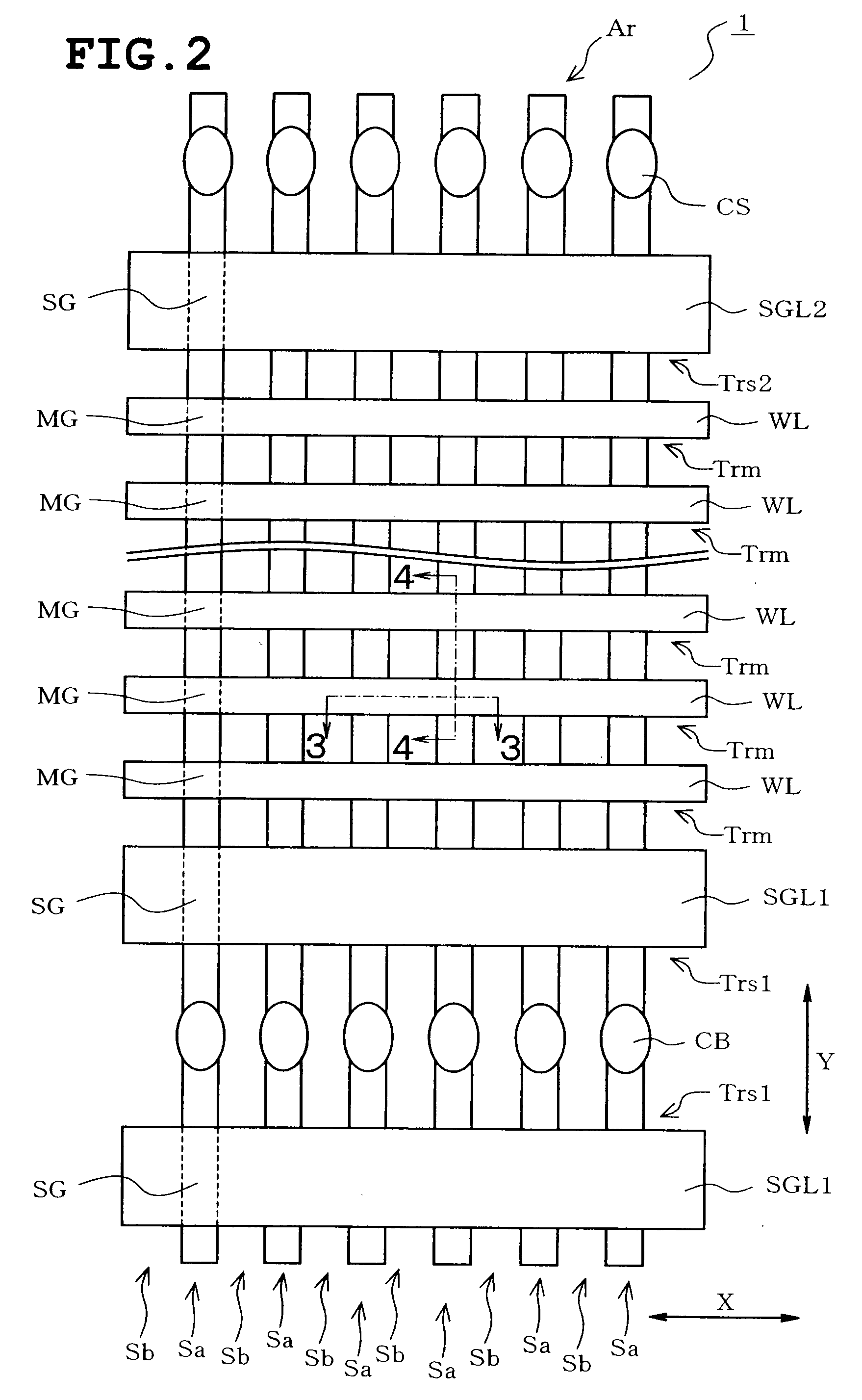
[0054]Referring to FIG. 1, an equivalent circuit of a part of a memory cell array Ar of a NAND flash memory 1 of the embodiment is shown. The memory cell array Ar includes a number of NAND cell units UC arranged in rows and columns. Each NAND cell unit UC includes two selective gate transistors Trs1 and Trs2 and a plurality of, for example, 32 memory cell transistors Trm series-connected between the selective gate transistors Trs1 and Trs2. The memory cell transistors Trm adjacent to each other have commonly used source / drain regions respectively.

[0055]The memory cell transistors Trm aligned in the X direction (...

second embodiment

[0078] damage due to atmosphere or heat is suppressed since the silicon nitride film 14 is formed between the metal oxide film 9 and the control gate CG. Consequently, an ideal composition or energy band state can be realized, which can improve the device characteristics.

[0079]The invention should not be limited by the foregoing embodiments. The embodiments can be modified or expanded as follows. The silicon nitride film 8 is formed between the silicon oxide film 7 and the metal oxide film 9 in each of the foregoing embodiments. However, any nitride-containing film may be used, instead of the silicon nitride film 8. For example, boron nitride (BN) or aluminum nitride (AlN) may be used.

[0080]The invention is applied to the NAND flash memory 1 in the foregoing embodiments. However, the invention may be applied to other types of semiconductor memory devices in which a number of memory cell transistors Trm are arranged in the bit line and word line directions into a matrix and data is c...

third embodiment

[0117]As described in the third embodiment, in the data erasing, the peripheral circuit applies low voltage (0 to 2.5 V, for example) to the word line WL corresponding to data to be erased and high voltage to the p-well 2b. As a result, electrons go through the floating gate electrode FG into the p-well 2b, whereby data is erased. In this case, since the electrons are injected from the conductive layer 18 into the floating gate electrode FG, there is a possibility that the threshold voltage of the memory cell transistor Trm in the data erasing may be saturated.

[0118]In view of the above-described problem, the embodiment provides a layer structure of the intergate insulating film 37 as shown in FIG. 38. The intergate insulating film 37 comprises a lower layer insulating film 37a, a high dielectric insulating film 37b serving as the intermediate insulating film and an upper layer insulating film 37c, all of which are deposited into a depositional structure. The lower insulating film 3...


PUM


Abstract

A nonvolatile semiconductor memory device includes a semiconductor substrate, a first insulation layer formed on the semiconductor substrate, a charge storage layer formed on the first insulation layer, a second insulation layer formed on the charge storage layer, a control electrode formed on the second insulation layer. The second insulation layer includes a first silicon oxide film, an intermediate insulating film formed on the first silicon oxide film and having a relative permittivity of not less than 7, and a second silicon oxide film formed on the intermediate insulating film. A charge trap layer is formed at least in either first or second silicon oxide film or a boundary between the first silicon oxide film and the intermediate insulating film or a boundary between the second silicon oxide film and the intermediate insulating film.

Description

CROSS-REFERENCE TO RELATED APPLICATIONS[0001]This application is based on and claims the benefit of priority from the prior Japanese Patent Application Nos. 2007-323317, filed on Dec. 14, 2007, 2008-8301, filed on Jan. 17, 2008, 2008-127125, filed on May 14, 2008, and 2008-136568, filed on May 26, 2008, the entire contents of all of which are incorporated herein by reference.BACKGROUND OF THE INVENTION[0002]1. Field of the Invention[0003]The present invention relates to a nonvolatile semiconductor memory device including a memory cell in which a charge storage layer and a control gate electrode are configured with an intergate insulating film being interposed therebetween and a method of fabricating the same.[0004]2. Description of the Related Art[0005]A conventional nonvolatile semiconductor memory device comprises a number of memory cells arranged in directions of word lines and bit lines for the purpose of achieving a higher degree of integration. With a recent tendency of higher...

Claims


Application Information

Patent Timeline
Patent Type & Authority Applications(United States)
IPC IPC(8): H01L29/792H01L21/28
CPCH01L27/115H01L27/11521H01L29/792H01L29/513H01L29/7881H01L27/11568H10B69/00H10B41/30H10B43/30
Inventor MATSUO, KAZUHIROTANAKA, MASAYUKIFURUHATA, TAKEONAKAHARA, KOJI
Owner KIOXIA CORP
Why Eureka
Try Eureka