Semiconductor package and method for making the same

a technology of semiconductors and packages, applied in semiconductor devices, semiconductor/solid-state device details, electrical apparatus, etc., can solve the problems of increased electricity consumption, signal rebounding, power loss, etc., and achieve the effect of reducing parasitic impedance and inductance value of the redistribution layer

Active Publication Date: 2009-06-18
ADVANCED SEMICON ENG INC
View PDF1 Cites 15 Cited by
  • Summary
  • Abstract
  • Description
  • Claims
  • Application Information

AI Technical Summary

Benefits of technology

[0008]The present invention provide a semiconductor package which is able to control the characteristic impedance of a high-speed and high-frequency IC chip with a redistribution layer. The present invention provides a semiconductor package which is able to reduce the parasitic impedance and the inductance value of the redistribution layer.

Problems solved by technology

However, when high speed and high frequency signals are transferred, the long and thin traces of the single-layered layout cannot steadily control the characteristic impedance, so a noise of power is produced and the signal is rebounded, which is the main disadvantage.
Moreover, when the numbers and the intensity of the devices in an IC chip increase, the consumption of electricity increases.
Although the redistribution layer redistributes the solder joint to the periphery, two sides or any side of the chip by the long and thin traces, it causes difficulty in heat dissipation, which increases the temperature of the chip and influences the characteristic and function of the chip.
Finally, it leads to lower yield rate of the chip, which is another disadvantage.
Therefore, redistributing the solder joint of the signal input and output terminal by the conventional redistribution layer with long and thin traces has the disadvantages of high parasitic impedance, lack of voltage, and uncontrolled characteristic impedance.

Method used


Image

  • Semiconductor package and method for making the same
  • Semiconductor package and method for making the same
  • Semiconductor package and method for making the same

Examples


Embodiment Construction

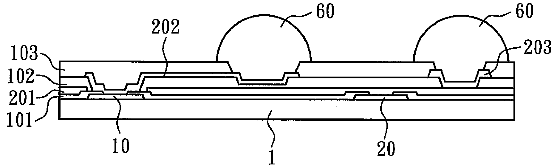
[0019]The semiconductor package and method for making the same of the present invention will be described by illustrating the following embodiments with reference to accompanying FIGS. 1 to 6. It should be noted that, “on” and “under” are used to illustrate the provisional position in the figures, not to limit the present invention.

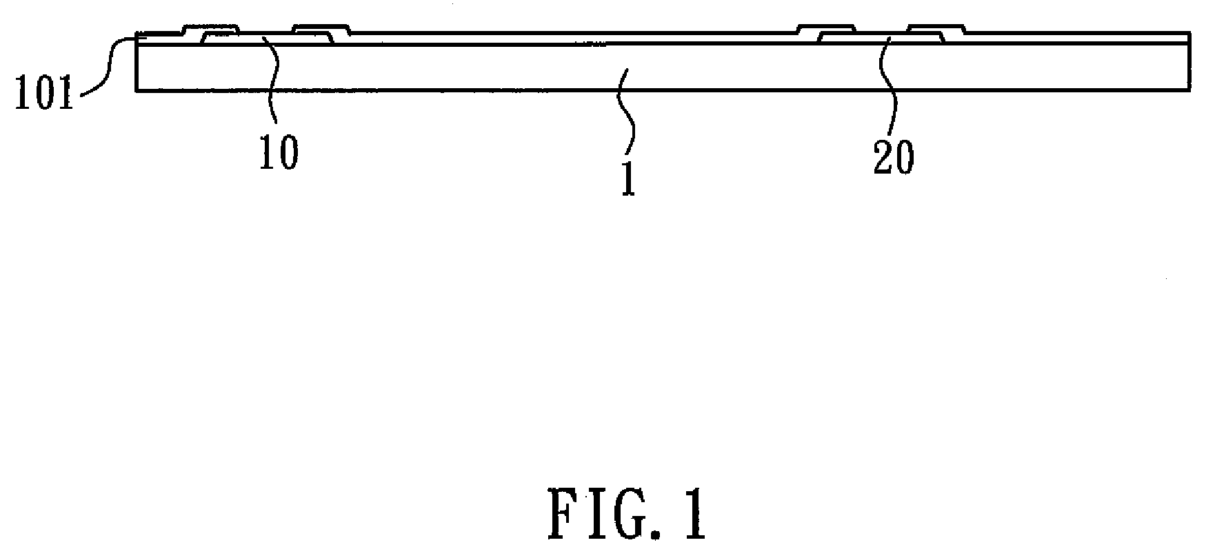
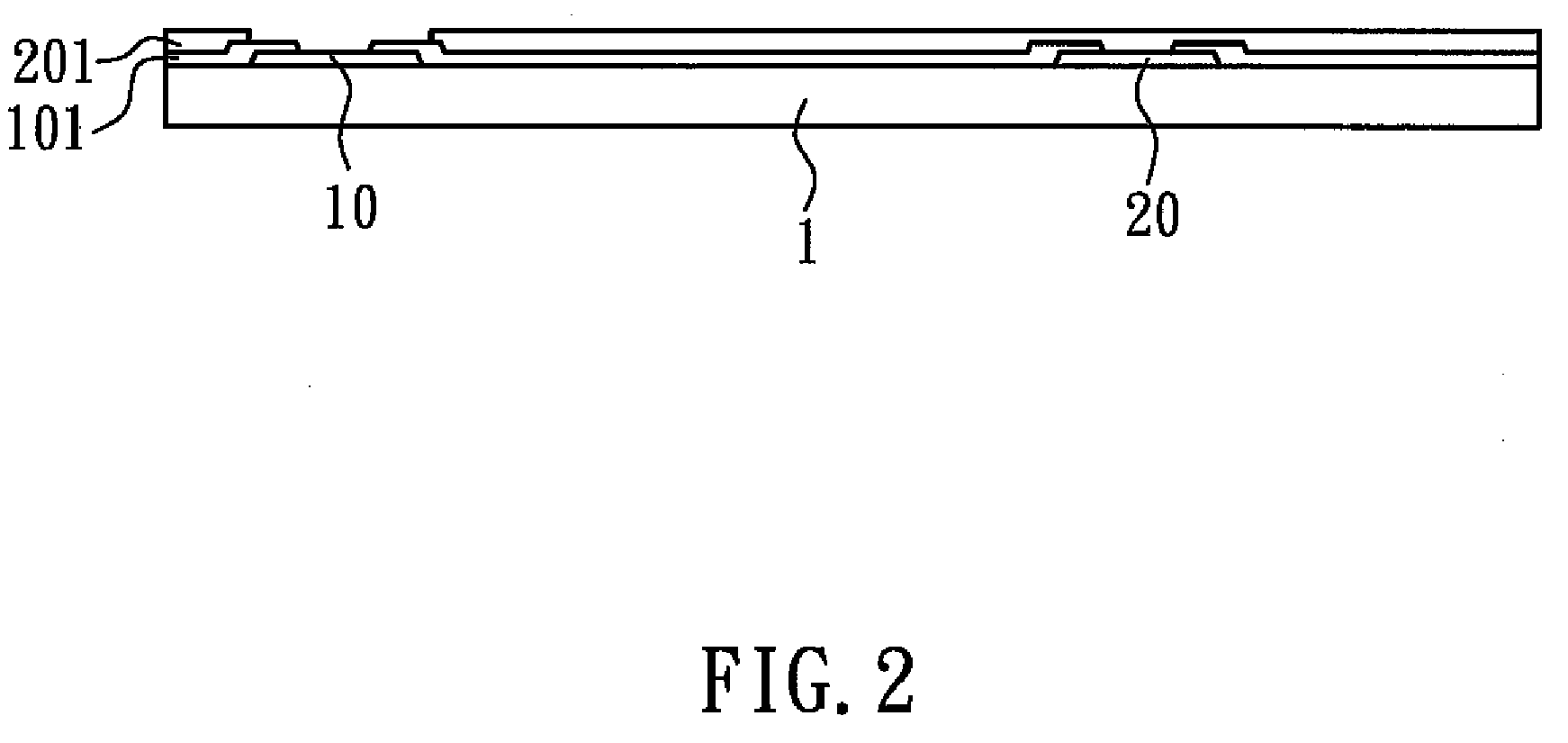
[0020]FIG. 1 shows a schematic view according to a method for making a semiconductor package of the present invention after a first passivation layer is formed. As shown in FIG. 1, a substrate 1, for example a wafer, is provided. The substrate 1 has a surface 100, which has at least one first pad 10 and at least one second pad 20 thereon. A first passivation layer 101 is then formed to cover the surface 100 of the substrate 1 and expose the first pad 10 and the second pad 20. The material of the first passivation layer 101 may be but is not limited to benzo-cyclo-butence or polyimide. The first pad 10 is a signal input and output terminal, and the second ...


PUM


Abstract

The present invention relates to a semiconductor package and a method for making the same. The semiconductor package includes a substrate, a first passivation layer, a first metal layer, a second passivation layer, a second metal layer and a third metal layer. The substrate has a surface having at least one first pad and at least one second pad. The first passivation layer covers the surface of the substrate and exposes the first pad and the second pad. The first metal layer is formed on the first passivation layer and is electrically connected to the second pad. The second passivation layer is formed on the first metal layer and exposes the first pad and part of the first metal layer. The second metal layer is formed on the second passivation layer and is electrically connected to the first pad. The third metal layer is formed on the second passivation layer and is electrically connected to the first metal layer.

Description

BACKGROUND OF THE INVENTION[0001]1. Field of the Invention[0002]The present invention relates to a semiconductor package and a method for making the same, and more particularly to a semiconductor package having a redistribution layer and a method for making the same.[0003]2. Description of the Related Art[0004]There is a tendency of making smaller and lighter electrical products, so packages with higher intensity of pins and new packaging methods are developed. Those new packaging methods include: (1) Ball Grid Array (BGA), which uses solder balls to replace conventional pins, the solder balls being connected to a circuit board and disposed in array, (2) Flip Chip, which places an active surface of a chip downward to connect the chip and the substrate by Sn / Pb bumps; (3) Quad Flat Package (QFP). Currently, the most advanced packaging technique is redistribution layer (RDL). In conventional packaging technique, a solder joint must go through the center of a chip. However, the redistr...

Claims


Application Information

Patent Timeline
Patent Type & Authority Applications(United States)
IPC IPC(8): H01L23/48H01L21/00
CPCH01L24/03H01L24/05H01L2924/0002H01L24/13H01L2224/0401H01L2224/05567H01L2224/13022H01L2924/01029H01L2924/0105H01L2924/01079H01L2924/01082H01L2924/014H01L2924/14H01L2924/30107H01L2924/3011H01L2924/01005H01L2924/01006H01L2924/01033H01L2924/01047H01L2224/05552H01L2224/023H01L2924/0001
Inventor HUANG, CHIH-YICHENG, HUNG-HSIANG
Owner ADVANCED SEMICON ENG INC
Why Eureka
Try Eureka