Picture element structure of current programming method type active matrix organic emitting diode display and driving method of data line

a technology of active matrix and driving method, which is applied in the direction of instruments, static indicating devices, etc., can solve the problems of deviation in oled output current, difficulty in manufacturing an ltps tft with such a desired uniformity, etc., and achieve the effect of increasing the output resistance of the fourth driving transistor

Active Publication Date: 2009-06-18
SEOUL NAT UNIV R&DB FOUND
View PDF15 Cites 51 Cited by
  • Summary
  • Abstract
  • Description
  • Claims
  • Application Information

AI Technical Summary

Benefits of technology

[0011] It is, therefore, an object of the present invention, with a view to overcome the aforementioned disadvantage, to provide the new structure of picture elements in a current programming type of active matrix organic light emitting diode (OLED) display. The structure makes it possible to compensate for OLED current deviations due to the deterioration in threshold voltage and uneven electrical characteristic in TFT elements between picture elements, thereby allowing the OLED picture elements to provide uniform light emitting characteristic.
[0012] It is another object of the present invention to provide the picture element structure in a current programming type of active matrix OLED display that makes it possible to enlarge a current control width per gray in a current data driver stage for controlling a current source, thanks to lowering the current scaling ratio as compared to the conventional structure of picture element.
[0019] a fifth transistor connected in series to the fourth driving transistor, for making an output resistance of the fourth driving transistor to increase.

Problems solved by technology

However, it is known from the state of the art that it is very difficult to manufacture an LTPS TFT with such a desired uniformity in threshold voltage and field effect mobility, which is usually processed under a low temperature environment of less than about 450° C. Therefore, various solutions have been so far sought to ensure the uniformity in TFT, with accesses in the side of physical circuits, for instance, among others, by providing a compensation circuit to each picture element in an active matrix OLED panel.
Accordingly, it is appreciated that in case where the OLED threshold voltage deteriorates as a panel operating time becomes longer, the aforementioned prior-art picture cell structure will have a disadvantage that it causes the deviation in OLED output current to occur owing to kink characteristic in TFT T4.

Method used


Image

  • Picture element structure of current programming method type active matrix organic emitting diode display and driving method of data line
  • Picture element structure of current programming method type active matrix organic emitting diode display and driving method of data line
  • Picture element structure of current programming method type active matrix organic emitting diode display and driving method of data line

Examples


first embodiment

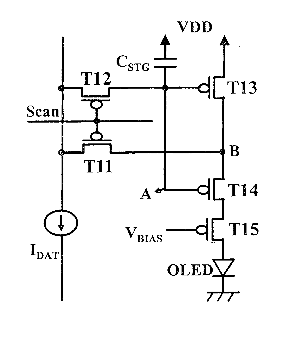
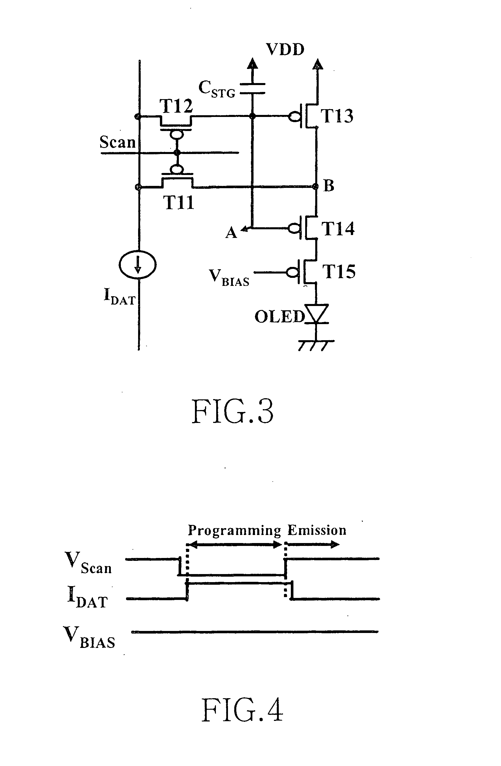
[0043]FIG. 3 schematically shows the structure of picture element in a current programming type of active matrix OLED according to the present invention, and then FIG. 4 shows a timing diagram of operation in FIG. 3. Referring now to FIG. 3, it is seen that the picture element in a current programming type of active matrix OLED according to the preferred embodiment of the present invention is configured to have five P-type thin film transistors (TFTs) T11 to T15 and a capacitor CSTG, in such a manner that a DC signal VBIAS in addition to a scan signal and a data signal IDATA, which are essential signals for the picture element, is further applied to a gate of TFT T15. It should be appreciated that this embodiment as described above also utilizes a characteristic that threshold voltages and field effect mobility in TFT T13 and TFT T14 are substantially identical to each other, as is with the current-mirror structure indicated in the known structure of FIG. 1. In a low temperature pol...

fourth embodiment

[0059]FIG. 11 schematically shows the picture element structure in a current programming type of active matrix OLED according to the present invention, and

[0060]FIG. 12 shows a timing diagram of operation in FIG. 11. As seen in FIG. 11, the picture element in a current programming type of active matrix OLED according to this embodiment includes five P-type TFTs T41 to T45 and a capacitor CSTG, as seen in the first embodiment of FIG. 3. Here, the difference in structure between this embodiment and the first embodiment of FIG. 3 is that two scan signals are applied to effect more stable circuit operation, so that TFT T41 is turned OFF earlier than TFT T42 in operation. This inventive idea of controlling a switching of two TFTs T41 and T42 using these two scan signals may be likewise applied to all the aforementioned embodiments of the present invention and any other alternative embodiments to be discussed in the following.

[0061]FIG. 13 schematically shows the picture element structur...

third embodiment

[0063] The basic concept that was applied to the preferred embodiments of FIGS. 13 and 15, for outputting the compensated OLED current by changing the physical position of TFT T2, may be also utilized for FIG. 9 according to the present invention.


PUM


Abstract

The present invention provides a novel structure of picture elements in current programming-type semiconductor devices, and in particular, the structure of picture elements of an active matrix organic light emitting diode (OLED) display. The device makes a self-compensation for OLED current deviations due to the deterioration in threshold voltage and uneven electric characteristic in thin film transistors. The invention also provides a method for driving a data driver capable of compensating for the uneven electric characteristic of thin film transistors in the driver for driving picture elements in the current programming-type active matrix OLED display device.

Description

[0001] The present invention relates generally to the structure of picture elements in an active matrix organic light emitting diode (OLED) display and, in particular, to the structure of current-programming type picture elements suitable for making a self-compensation for current deviation in OLED resulting from the deterioration in a threshold voltage of OLED and non-uniform electric characteristic in thin film transistors. BACKGROUND ART [0002] It is so far known from the state of the art that an active matrix liquid crystal display (LCD) using a low temperature polycrystalline silicon thin film transistor (LTPS-TFT) generally provides better driving capability and higher degree of integration than a display adopting amorphous silicon thin film transistors (a-Si TFT) currently in wide use for monitors of notebook computers and desktop personal computers. Thanks to such an advantage, the active matrix LCDs tend to be more frequently adopted for a high resolution LCD device. [0003]...

Claims


Application Information

Patent Timeline
Patent Type & Authority Applications(United States)
IPC IPC(8): G09G3/36
CPCG09G3/3241G09G2300/0819G09G2320/043G09G2310/0224G09G2320/0252G09G2300/0842
Inventor HAN, MIN-KOOLEE, JAE-HOONNAM, WOO-JIN
Owner SEOUL NAT UNIV R&DB FOUND
Why Eureka
Try Eureka