
Floating body control in soi dram

a floating body control and memory device technology, applied in static storage, information storage, digital storage, etc., can solve the problems of parasitic floating body effects, loss of information from memory cells, and high current consumption

Inactive Publication Date: 2009-06-18
GLOBALFOUNDRIES INC
View PDF6 Cites 5 Cited by
  • Summary
  • Abstract
  • Description
  • Claims
  • Application Information

AI Technical Summary

Benefits of technology

[0032]the control logic adapted to generate the body refresh cycle periodically wherein the voltage supplied to the first word line is deactivated while the bit line and bit line bar voltages continue, and the control logic is adapted to re-activate

Problems solved by technology

The charge accumulates on the capacitor and may cause adverse effects, such as, opening of parasitic transistors in the structure and causing off-state leakages, resulting in higher current consumption and in case of a DRAM cell, loss of information from the memory cells.
Thus, parasitic floating-body effects are generally associated with partially depleted transistors.
Typically, high performance DRAM cells with SOI access transistors have a high leakage rate and thereby lose data through sub-threshold leakage.
As a result, a ground (GND) pre-charge scheme that keeps the BL / BLB (bit line, and bit line bar) at GND during a retention period will destroy high data (logic 1) on the DRAM cell node.
This results in high leakage current when the bit line or bit line bar (reference bit line) is pulled down (reduced to zero).
The occurrence of high current leakage may result in data destruction.
This scenario results in continuous leakage and results in lower data retention time.
This leads to destruction of the stored data because the increased floating body increases channel leakage.
However, both GND and VDD pre-charge schemes increase the body potential and lead to short retention of data.
Thus, data in a typical DRAM cell is susceptible to leakage resulting in loss of data.

Method used


Image

  • Floating body control in soi dram
  • Floating body control in soi dram
  • Floating body control in soi dram

Examples


Embodiment Construction

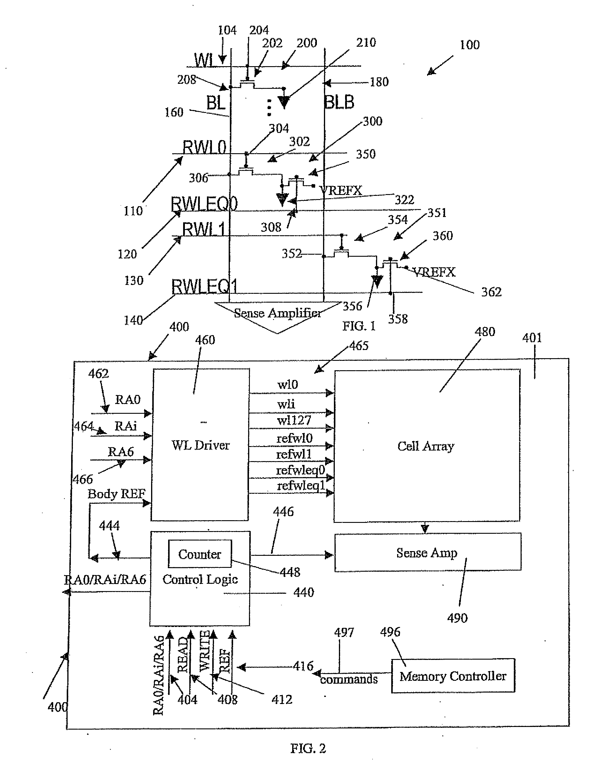
[0040]An embodiment of the present invention is described herein with reference to the accompanying drawings. In general, transistors used in the embodiment described herein may be formed on a single semiconductor substrate such as that made of a single crystal silicon by known integrated circuit technologies such as a CMOS transistor (complementary metal-oxide semiconductor) and the like, or silicon on insulator (SOI) techniques.

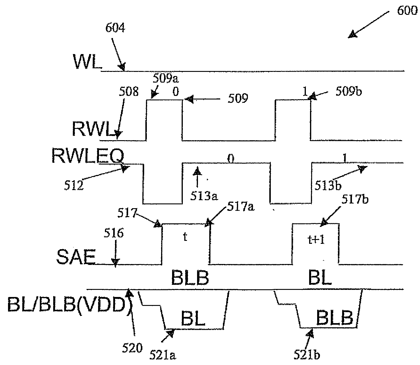
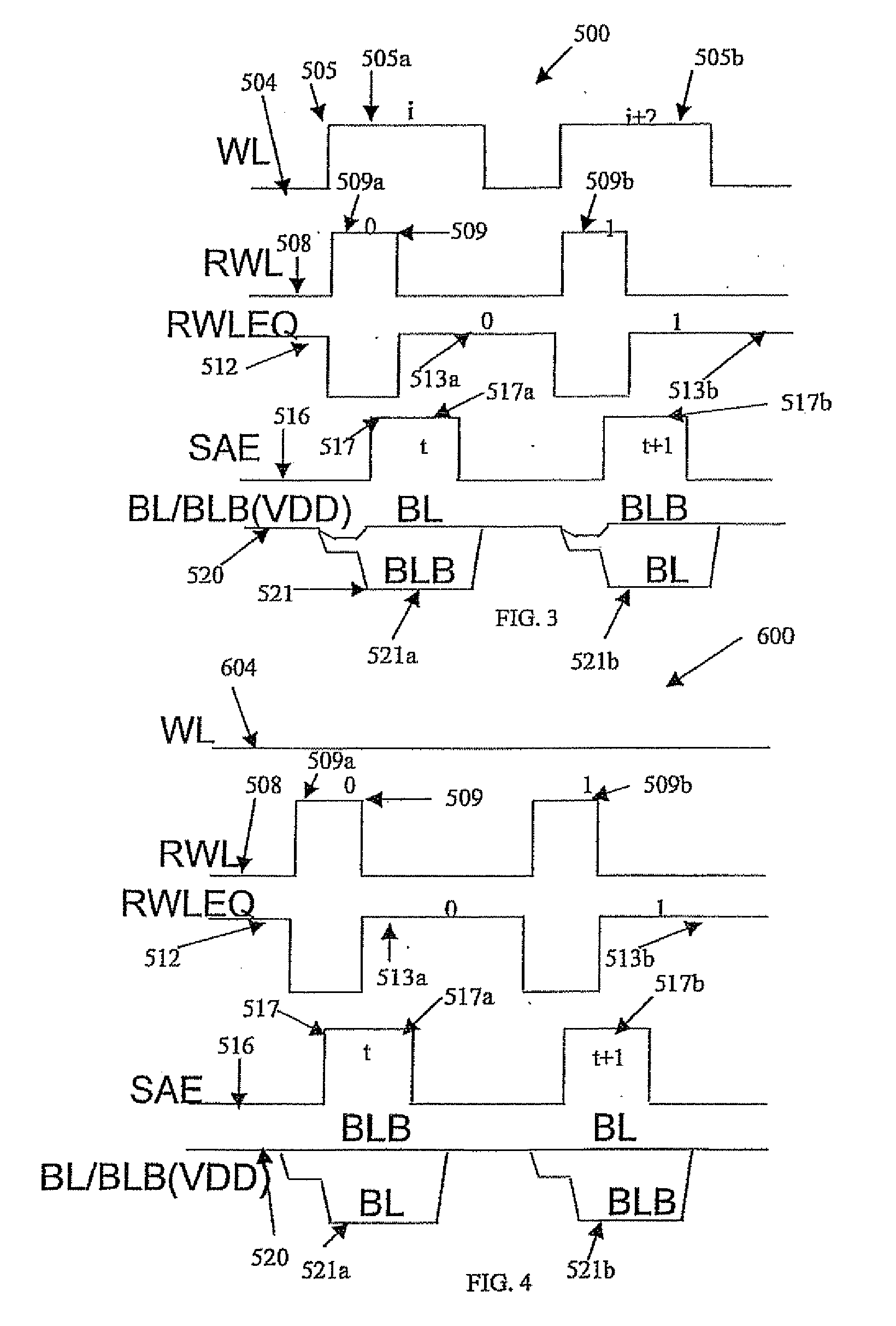
[0041]The present invention provides a system and method for implementing a floating body refresh cycle for a VDD or VDD / 2 (half of the VDD) pre-charge scheme. The present invention may be used with high leakage, high performance silicon on insulator (SOI) dynamic random access memory (DRAM) cell design. A DRAM cell typically has a read / write operation and a data refresh operation. The present invention adds a body refresh operation whereby the floating body is refreshed. When the floating body is not refreshed and the voltage is maintained at a specified a...


PUM


Abstract

A system including a DRAM memory device on an integrated circuit (IC) using a control logic device to initiate a body refresh operation to provide a means for maintaining a low voltage at a floating body and discourage data loss, and a design structure including the DRAM memory device embodied in a machine readable medium is provided. A plurality of DRAM cells are connected to a first word line circuit and a first bit line circuit. The control logic device is coupled to the DRAM memory device and the IC for initiating the body refresh cycle. The control logic communicates with a first bit line and word line circuits and communicates with a reference word line and bit line circuits. A sense amplifier circuit and signal is provided for amplifying the voltage at the first bit line and the reference bit line. The body refresh cycle includes deactivating the first word line voltage while the first bit line and reference bit line voltages continue.

Description

RELATED APPLICATION[0001]This application is related to co-pending and co-assigned U.S. patent application Ser. No. 11 / 534,070, filed Sep. 21, 2006, currently pending.FIELD OF THE INVENTION[0002]The present invention relates to semiconductor memory devices, and more particularly, to a dynamic random access memory (DRAM) device having an SOI (Silicon On Insulator) structure in which a memory cell is formed on an insulation layer, and a design structure including the DRAM device embodied in a machine readable medium.BACKGROUND OF THE INVENTION[0003]Currently, semiconductor dynamic random access memory (DRAM) memory devices are available for silicon on insulator SOI and for complementary metal-oxide semiconductor (CMOS) integrated circuits (IC)s. An SOI type thin film transistor is used as a component in three-dimensional integrated circuits and liquid crystal displays. The SOI type thin film transistor includes a power source / drain region or active region formed at a semiconductor Lay...

Claims


Application Information

Patent Timeline
IPC IPC(8): G11C7/00
CPCG11C11/406G11C2211/4065G11C2211/4016
Inventor KIM, HOKIWANG, GENG
Owner GLOBALFOUNDRIES INC
Learn More