Processor memory system

a memory system and processor technology, applied in the field of processor memory systems, can solve the problems of increasing delay and complexity, types of access allowed, etc., and achieve the effects of simplifying inter-processor communication, facilitating compiler optimisation, and simplifying memory usag

Inactive Publication Date: 2009-06-25
RAMBUS INC
View PDF2 Cites 27 Cited by
  • Summary
  • Abstract
  • Description
  • Claims
  • Application Information

AI Technical Summary

Benefits of technology

[0021]The invention simplifies inter-processor communications within a SIMD array and also unifies mono and poly memory into a single address space. This greatly simplifies memory usage for the programmer and expands the potential for compiler optimisation. It also combines the performance benefits of local PE memory and the ease of use of shared memory. The invention also increases the efficiency of operation of a SIMD processor when inter-PE communications and computation are mixed within a program.

Problems solved by technology

Certain problems with previous implementations of shared memory SIMD can be identified as follows, in that they:a require complex and non-scalable cross-bar or multi-port memory systems;use central arbitration of accesses to memory, adding delay and complexity;often limit the types of access allowed: e.g. all PEs access a fixed offset.

Method used


Image

  • Processor memory system
  • Processor memory system
  • Processor memory system

Examples


Embodiment Construction

[0054]The invention will now be described with reference to the following drawings, in which:

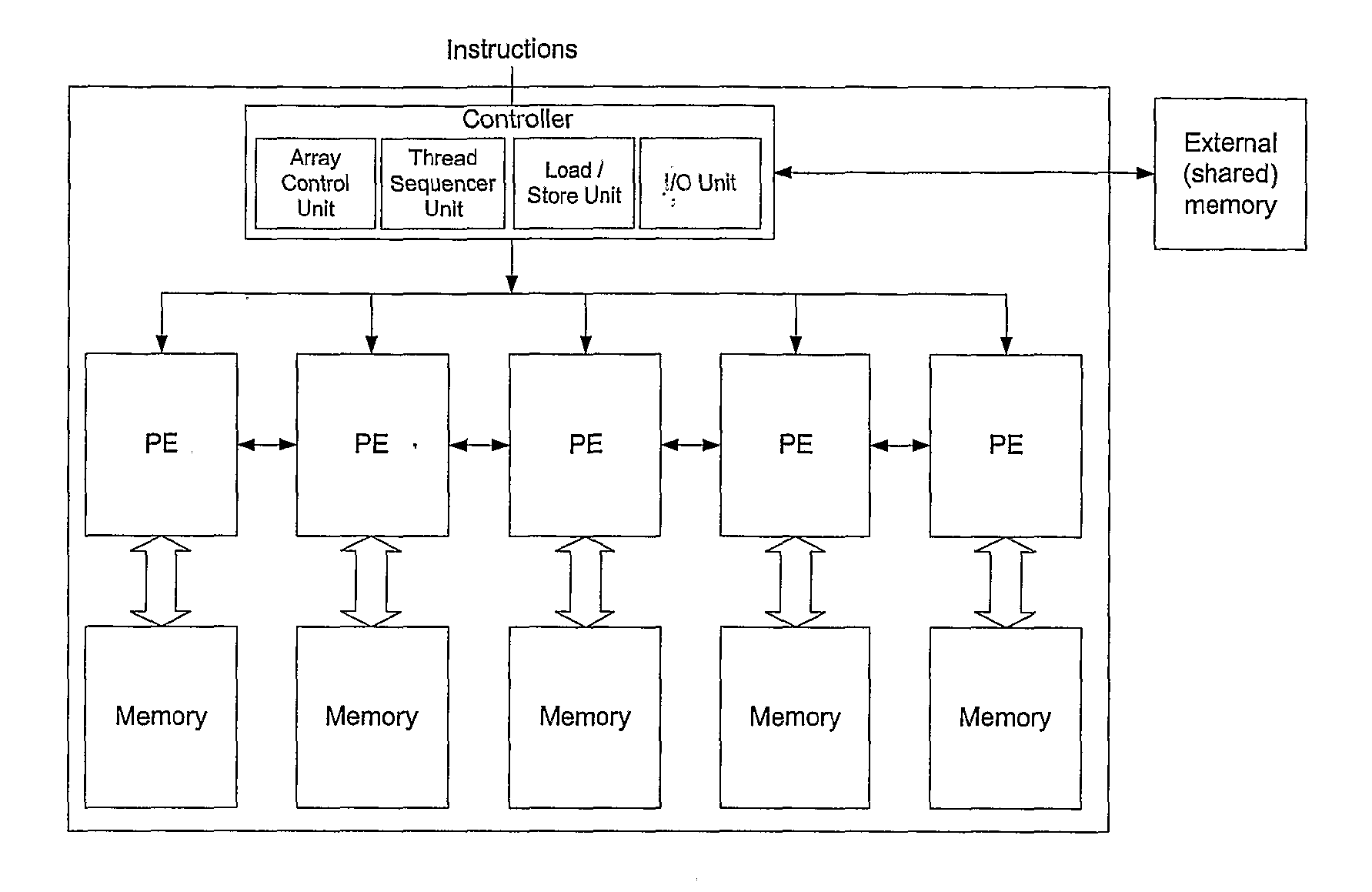
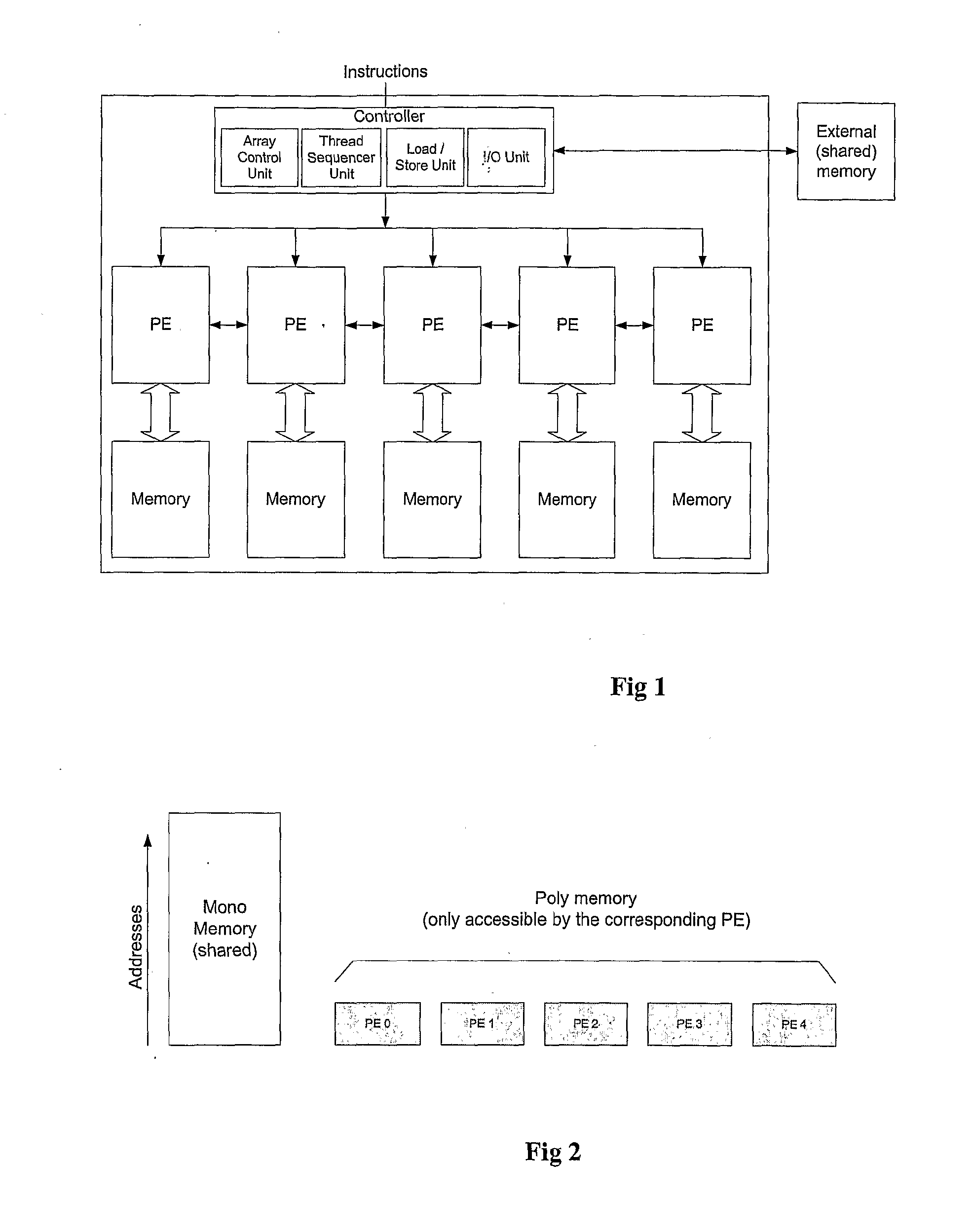
[0055]FIG. 1 illustrates a traditional SIMD architecture;

[0056]FIG. 2 illustrates schematically separate poly and mono memory maps;

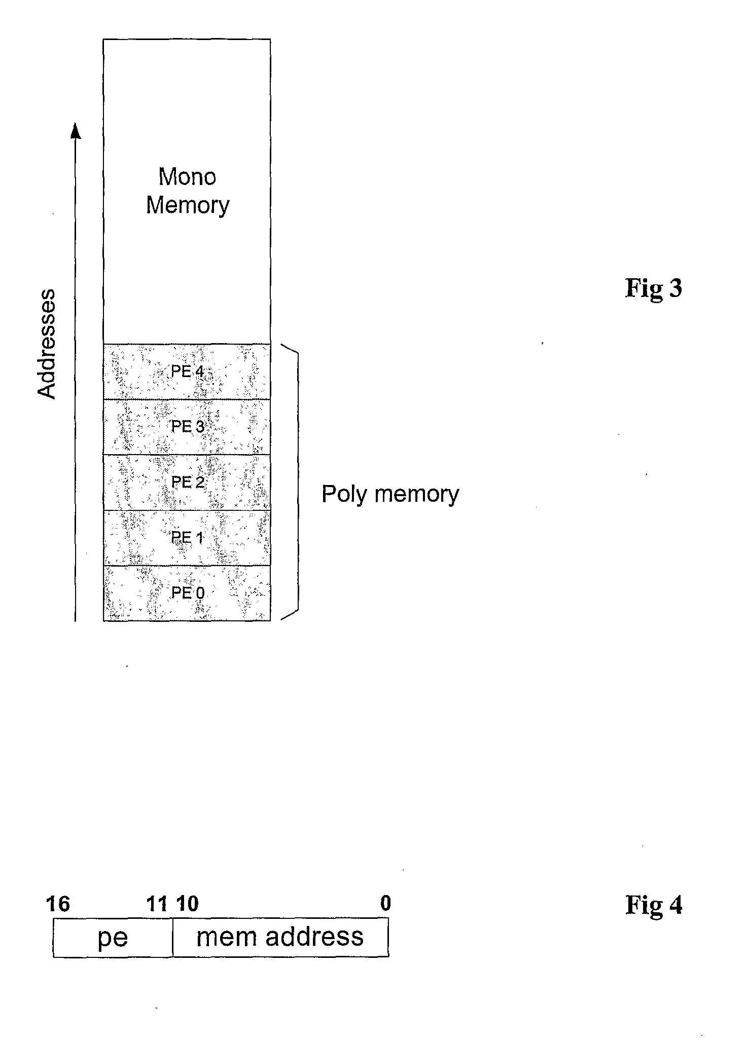
[0057]FIG. 3 illustrates schematically an address map for unified memory, showing how to generate shared memory address from PE id and memory address for an example of 2K word memory (11 bit addresses) and 64 PEs (6 bit PE number);

[0058]FIG. 4 shows how to generate shared memory address from PE id and memory address;

[0059]FIG. 5 illustrates an address map for virtualised PE memory;

[0060]FIG. 6 is a schematic diagram of a CCB interconnecting PE memories;

[0061]FIG. 7 illustrates the operation of inter-PE transfers, routing requests between PE registers and memory:

[0062]FIG. 8 illustrates the operation of Concurrent transfers:

[0063]FIG. 9 illustrates an example of the invention using an intermediate end node; and

[0064]FIG. 10 illustrates a shared load / store unit use...


PUM


Abstract

A data processor comprises a plurality of processing elements (PEs), with memory local to at least one of the processing elements, and a data packet-switched network interconnecting the processing elements and the memory to enable any of the PEs to access the memory. The network consists of nodes arranged linearly or in a grid, e.g., in a SIMD array, so as to connect the PEs and their local memories to a common controller. Transaction-enabled PEs and nodes set flags, which are maintained until the transaction is completed and signal status to the controller e.g., over a series of OR-gates. The processor performs memory accesses on data stored in the memory in response to control signals sent by the controller to the memory. The local memories share the same memory map or space. External memory may also be connected to the “end” nodes interfacing with the network, eg to provide cache. One or more further processors may similarly be connected to the network so that all the PE memories from all the processors share the same memory map or space. The packet-switched network supports multiple concurrent transfers between PEs and memory. Memory accesses include block and/or broadcast read and write operations, in which data can be replicated within the nodes and, according to the operation, written into the shared memory or into the local PE memory.

Description

BACKGROUND TO THE INVENTION[0001]The present invention concerns processor (eg data processor) systems with enhanced inter-communication and memory arrangements.[0002]Current implementations of SIMD processors have local memory for each processing element (PE). This memory is normally private to each PE. In order to share data, the PEs either have to access data in a common shared memory or use some sort of inter-PE communication mechanism. Having two different types of memory complicates the programming model. Having to move data to shared memory, or between PEs, is a performance overhead.[0003]The object of the present invention is to overcome these and other problems.PRIOR ART[0004]Various classes of architecture, including SIMD architectures with shared memory are already known. A summary of some of these can be found at http / / www.top500.org / ORSC / 2003 / architecture.html. Two types in particular are worth referring to:[0005]Distributed memory systems: In this case each PE has its o...

Claims


Application Information

Patent Timeline
Patent Type & Authority Applications(United States)
IPC IPC(8): G06F15/80G06F9/06G06F9/312G06F9/38G06F15/173
CPCG06F15/17337G06F9/46G06F11/3017G06F15/8015G06F13/1657G06F12/109G06F2212/657
Inventor MCCONNELL, RAY
Owner RAMBUS INC
Why Eureka
Try Eureka