Oxide semiconductor device and surface treatment method of oxide semiconductor

a surface treatment method and semiconductor technology, applied in the direction of semiconductor devices, basic electric elements, electrical apparatus, etc., can solve the problems of difficult control of stoichiometric amount, difficult application of large-scale fpds in the future in view of process throughput problems, and difficult operation of display devices, etc., to achieve the effect of reliable operation of flexible devices, flexible devices and other devices

Inactive Publication Date: 2009-07-02
HITACHI LTD
View PDF7 Cites 364 Cited by
  • Summary
  • Abstract
  • Description
  • Claims
  • Application Information

AI Technical Summary

Benefits of technology

[0015]The reliability in the operation of display devices, RFID tags, flexible devices and other devices for which the other oxide semiconductors are applied can be improved by suppressing the threshold potential shift, occurrence of leak current due to oxygen defects present at the boundary between the oxide semiconductor and the gate insulator, and degradation of characteristics due to envelopment.

Problems solved by technology

For example, in a-Si used mainly for the switching of existent liquid crystal displays, since the shift of the threshold potential greatly exceeds the level of about 2 V which can be controlled easily by a compensation circuit, it is considered difficult to be applied as a thin-film transistor for the organic EL device.
Further, while polysilicon applied to small-to-medium sized displays has sufficient characteristics for driving organic EL device, it is difficult to be applied to large-scale FPDs in the future in view of a problem of process throughput.
In particular, while various studies have been made mainly on zinc oxide type oxide semiconductors, it has been known for zinc oxide that control for the grain boundary due to the presence of rotational domains during film formation or control for stoichiometrical amount is difficult, and oxygen defects are present.
The oxygen defects cause lowering of mobility, shift of threshold potential, leak current, etc. as sites for supplementing electrons and involve a problem not capable of taking the advantage inherent in wide gap oxide semiconductors.
Then, while amorphous type oxide semiconductor materials such as a-IGZO capable of suppressing the threshold potential shift have also been proposed, since they use rare metals of indium and gallium the cost of which has been increased in recent years, they involve a problem in view of the resource.
Further, indium also involves a problem of health hazard as an element causing interstitial pneumonia, it leaves a problem in the future application.

Method used


Image

  • Oxide semiconductor device and surface treatment method of oxide semiconductor
  • Oxide semiconductor device and surface treatment method of oxide semiconductor
  • Oxide semiconductor device and surface treatment method of oxide semiconductor

Examples


first embodiment

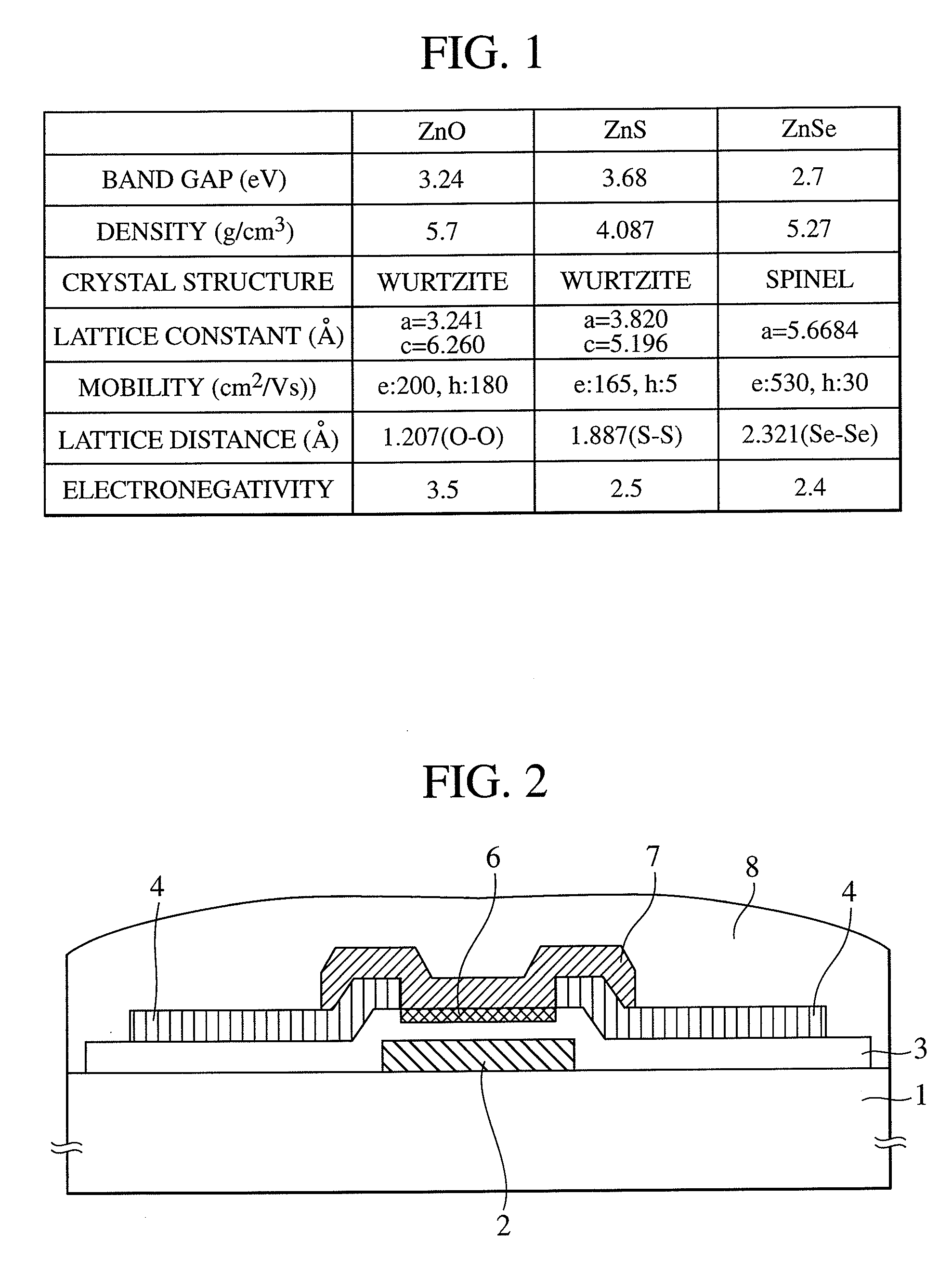
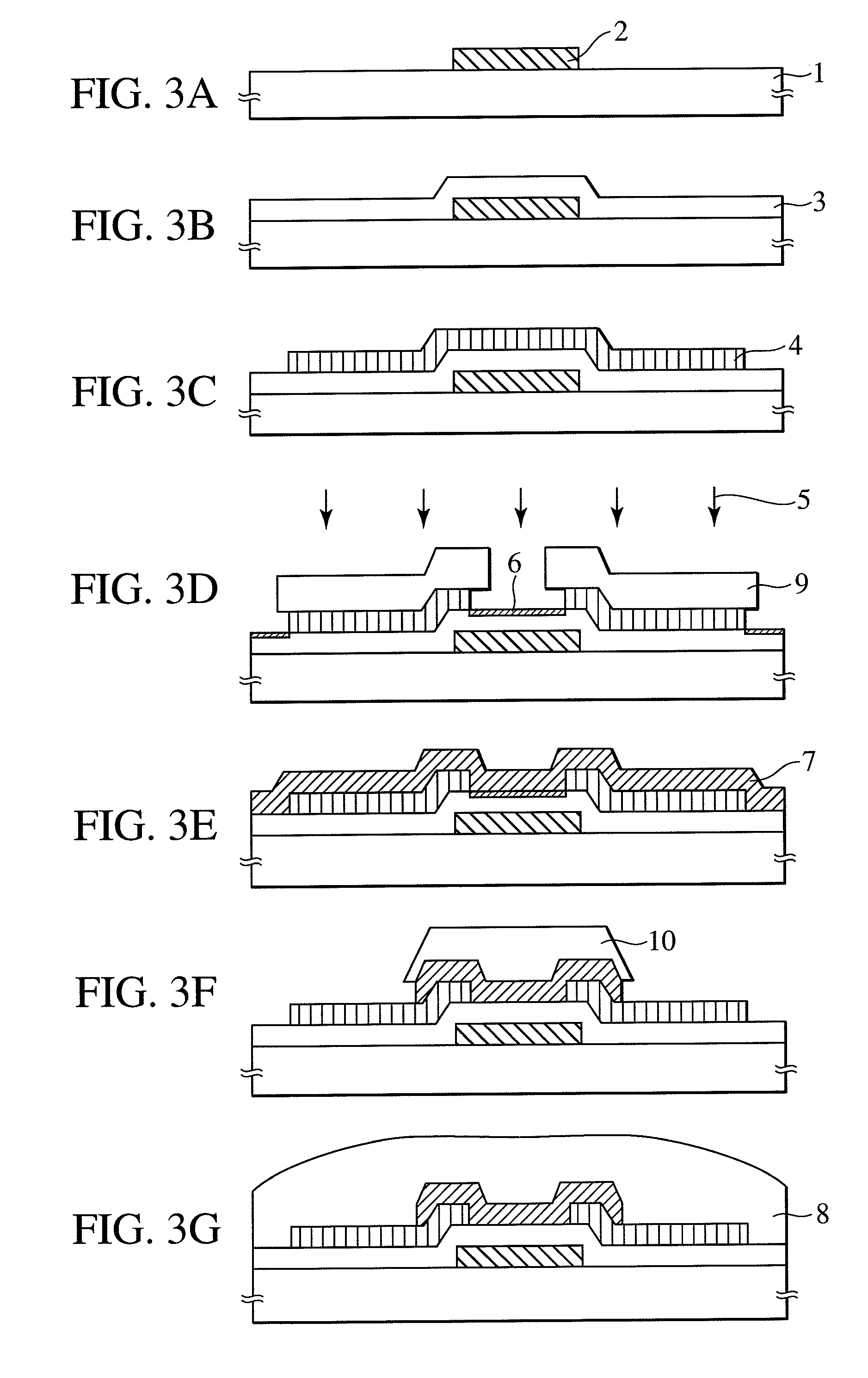
[0029]A structure of a thin-film transistor used for display and a manufacturing method according to a first embodiment of the invention are to be described with reference to FIG. 2 to FIG. 5. FIG. 2 and FIG. 3 are flow charts showing an example of cross sectional views of bottom gate type thin-film transistor and manufacturing steps thereof. FIG. 4 and FIG. 5 are flow charts showing an example of cross sectional views of top gate type thin-film transistor and manufacturing steps thereof. FIG. 6 and FIG. 8 are graphs for explaining the change with time of a threshold potential shift for showing respective effects. FIG. 7 and FIG. 9 are simple schematic views of circuits for applying them to devices respectively.

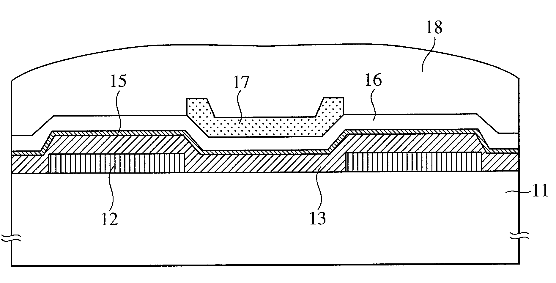
[0030]First, when a bottom gate type thin-film transistor as shown in FIG. 2 is formed, a support substrate 1, for example, a glass substrate is provided. Then, a metal thin-film as a gate electrode 2, for example, a lamination film of Al (250 nm) and Mo (50 nm) is formed by ...

second embodiment

[0039]Description is to be made to the structure of an HEMT (High Electron Mobility Transistor) and a manufacturing method according to a second embodiment of the invention with reference to FIG. 10.

[0040]First, a combination of a band structure so as to form a two dimensional electron gas layer 22 is selected and, for example, a multi-layer film 23 comprising, for example, zinc magnesium oxide / zinc oxide / zinc magnesium oxide is grown crystallographically by an MBE method or an MO (metal Organic) CVD method, a PLD (Pulsed Laser Deposition) method or the like above a semiconductor substrate 21 such as a sapphire substrate or a zinc oxide substrate. When the effect due to a substrate material or a polar surface is controlled, a buffer layer such as a zinc oxide layer or a zinc magnetic oxide layer grown on the surface of a semiconductor substrate at a low temperature condition of 200° C. or lower is sometimes disposed between the multi-layer structure 23 and the substrate 21. A gate i...


PUM


Abstract

Oxygen defects formed at the boundary between the zinc oxide type oxide semiconductor and the gate insulator are terminated by a surface treatment using sulfur or selenium as an oxygen group element or a compound thereof, the oxygen group element scarcely occurring physical property value change. Sulfur or selenium atoms effectively substitute oxygen defects to prevent occurrence of electron supplemental sites by merely applying a gas phase or liquid phase treatment to an oxide semiconductor or gate insulator with no remarkable change on the manufacturing process. As a result, this can attain the suppression of the threshold potential shift and the leak current in the characteristics of a thin film transistor.

Description

CLAIM OF PRIORITY[0001]The present application claims priority from Japanese patent application JP 2007-333865 filed on Dec. 26, 2007, the content of which is hereby incorporated by reference into this application.BACKGROUND OF THE INVENTION[0002]1. Field of the Invention[0003]The present invention relates to an oxide semiconductor device and a surface treatment method thereof and it particularly relates to a technique of improving the reliability of a thin-film transistor which is utilized as a switching device for liquid crystal televisions and organic EL televisions, a driver device and a basic element for RFID (Radio Frequency Identification) tags.[0004]2. Description of the Related Arts[0005]In recent years, display devices have been developed rapidly from displays using a cathode-ray-tube to a flat type display device referred to as a flat panel display (FPD) such as a liquid crystal panel and a plasma display panel. In liquid crystal panels, a-Si or polysilicon thin-film tran...

Claims


Application Information

Patent Timeline
Patent Type & Authority Applications(United States)
IPC IPC(8): H01L29/78H01L21/02
CPCH01L29/7869H01L27/1225H01L29/4908H01L29/78696
Inventor UCHIYAMA, HIROYUKI
Owner HITACHI LTD
Why Eureka
Try Eureka