Circuit device having a free wheeling diode, circuit device and power converter using diodes

a diode and circuit device technology, applied in the direction of diodes, electronic switching, pulse technique, etc., can solve the problems of increasing the switching loss, difficult to largely reduce the recovery current in the current state, and the carrier stored in the diode to be discharged

Inactive Publication Date: 2009-07-02
HITACHI LTD
View PDF7 Cites 65 Cited by
  • Summary
  • Abstract
  • Description
  • Claims
  • Application Information

AI Technical Summary

Problems solved by technology

A current diode has a problem with such a recovery current as to cause carriers stored in the diode to be discharged when the IGBT is turned ON.
The recovery current also involves another noise problem of increasing a switching loss.
Since the characteristic of the Si-PND already reaches nearly such a high level as to be determined by the material physical properties, however, it is difficult to largely reduce the recovery current in the current state.
Further, since the SBD is a unipolar device, the SBD can have a very small recovery current when the IGBT is turned ON.
However, the recovery current becomes nearly zero, which results in that a current abruptly varies and this causes generation of switching nose based on the resonance between a capacitance component and an inductance component in the circuit.
Noise may cause not only the destruction of the element but also a trouble in the entire system.
Further, since a current larger than the PND cannot be passed through the SBD element, a momentary large current called a surge may cause the SBD to be destroyed.
However, the PND also has a disadvantage that a reverse current causes generation of a (reverse bias) recovery loss.
The reverse bias recovery loss becomes large in a high voltage current and a high voltage converter circuit has a problem with a diode loss and with heat generation caused by the loss.
In a device including the MPS st

Method used


Image

  • Circuit device having a free wheeling diode, circuit device and power converter using diodes
  • Circuit device having a free wheeling diode, circuit device and power converter using diodes
  • Circuit device having a free wheeling diode, circuit device and power converter using diodes

Examples


first embodiment

1. First Embodiment

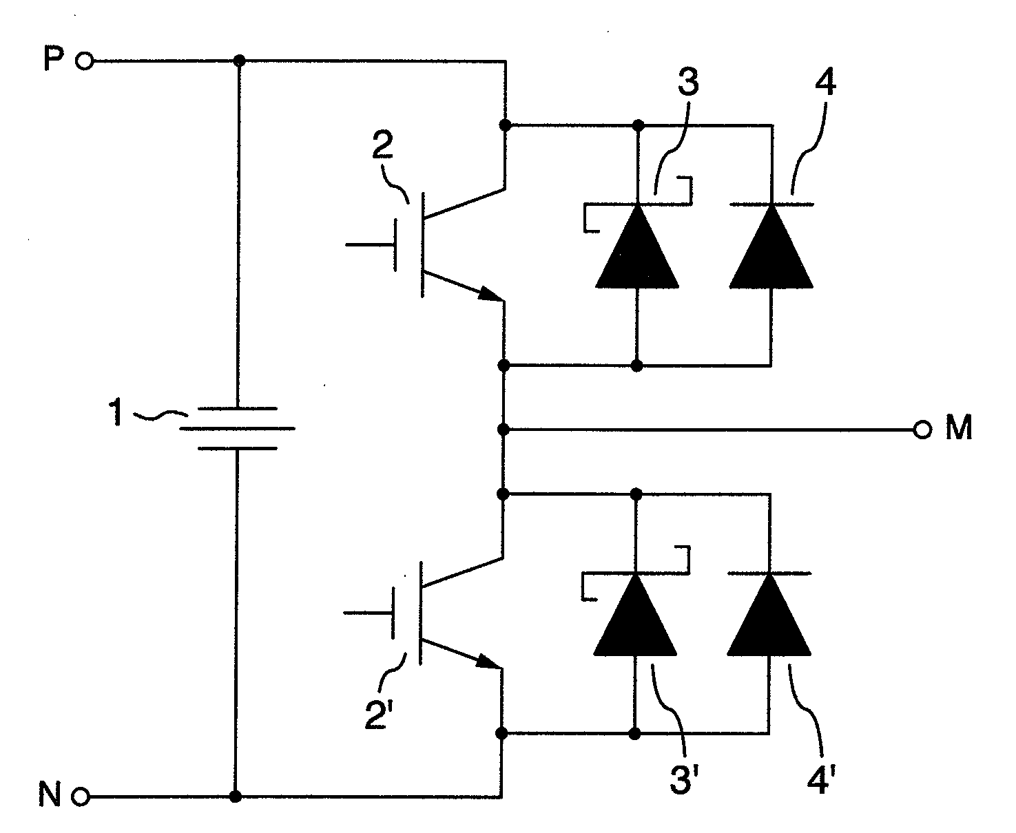
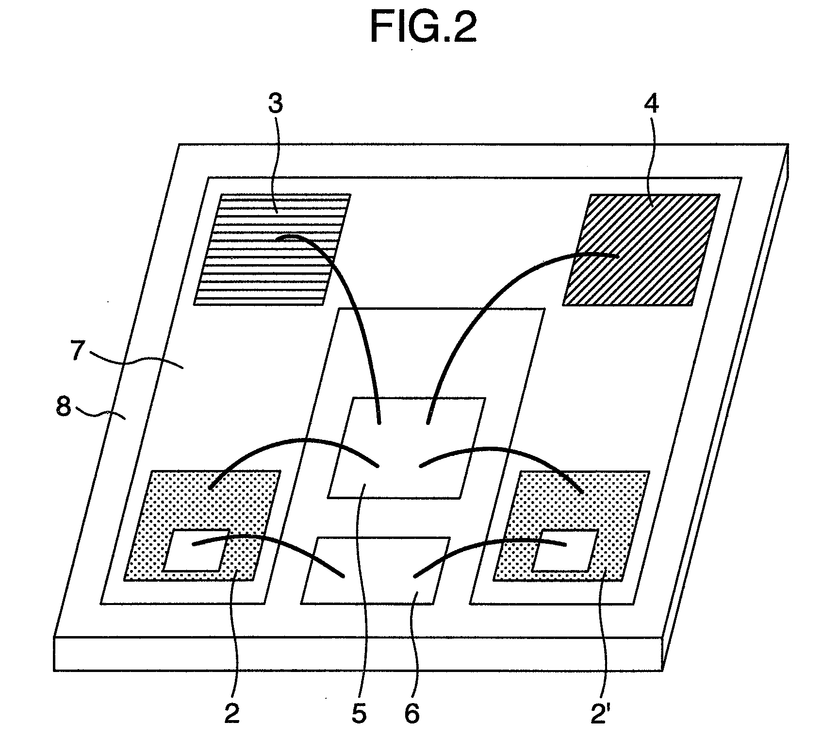
[0056]Explanation will first be made as to the first embodiment. The present embodiment is directed to a circuit device which includes at least one switching element and at least one free wheeling diode connected in parallel thereto, wherein a Schottky barrier diode and a silicon PiN diode having a semiconductor material with a band gap larger than silicon as a base material are connected in parallel, and the Schottky barrier diode and the silicon PiN diode are provided in the form of separate chips. The semiconductor material having a band gap larger than silicon is made of silicon carbide (SiC) as a typical example. The semiconductor material may also be made of gallium nitride (GaN). The free wheeling diode plays a role of holding a characteristic voltage and passing a current necessary for a load when the switching element is turned OFF by smoothing an abrupt variation in a circuit caused by the switching operation of the switching element, that is, plays a ro...

second embodiment

2. Second Embodiment

[0064]A second embodiment will next be explained.

[0065]The present embodiment is directed, as an example, to a circuit device which includes at least one switching element and a free wheeling diode connected in parallel to the switching element, wherein the free wheeling diode is made up of a Schottky barrier diode having a base material with a band gap larger than silicon and two or more PiN diodes connected in series therewith, the PiN diode uses a semiconductor material having a band gap larger than silicon as its base material, and the Schottky barrier diode and the PiN diode are provided in the form of separate chips.

[0066]FIG. 7 shows part of an inverter circuit to which a power module is applied in the second embodiment. FIG. 7 is different from the example of FIG. 1 in two first and second respects, that is, in that (1), as the first respect, a PiN diode made of a semiconductor material having a band gap larger than silicon is used in place of the PiN dio...

third embodiment

3. Third Embodiment

[0069]The arrangement of a converter circuit in accordance with a third embodiment of the present invention will be explained by referring to the drawings.

[0070]FIG. 10 shows a basic circuit in the arrangement of the converter circuit of the present invention. In FIG. 10, the basic circuit includes a first switching element 201, a first Schottky diode 202, a first capacitance 203, a first resistance 204, a positive side inductance 205, an AC terminal 206, a circuit positive terminal 207, a circuit negative terminal 208, a switching element 211 for the first Schottky diode 202, a second Schottky diode 212, a second capacitance 213, a second resistance 214, and a negative side inductance 215.

[0071]The circuit of the present embodiment will be explained with reference to FIG. 10.

[0072]FIG. 10 shows a basic circuit of a combination of the diodes and the switching elements forming the converter circuit. A combination of such basic circuits is used as a converter circui...


PUM


Abstract

A circuit device includes at least one switching element and a free wheeling diode connected in parallel to the switching element. The free wheeling diode is made up of a Schottky barrier diode using a semiconductor material having a band gap larger than silicon as its base material and also a silicon PiN diode, which are connected in parallel. The Schottky barrier diode and the silicon PiN diode are provided in the form of separate chips. A circuit system is also provided wherein a diode having a Schottky junction of a compound semiconductor as a rectification element built therein is combined, and a relationship, R2>4L/C, with impedance R (resistance), L (inductance), and C (capacitance) determined by a closed circuit between a power source and a positive or negative terminal when the current of the diode becomes zero during recovery operation, is satisfied.

Description

BACKGROUND OF THE INVENTION[0001]The present invention relates to a circuit device having at least one switching element and at least one free wheeling diode connected in parallel with the switching element, a circuit and a circuit mounting system for a system of a power converter such as an inverter or a converter.[0002]A semiconductor power module is used as a constituent element forming an inverter in a wide range of fields. In particular, a power module, using a Si-IGBT (Insulated Gate Bipolar Transistor) as a switching element and also using a Si-PiN diode (which will be referred to as the PND hereinafter) as a free wheeling diode, is high in breakdown voltage and low in loss. Such a power module is used in a wide range of fields including railroad and home appliances. In recent years, power saving becomes more important and the power module is required to further reduce its loss. The loss of the power module is determined by the performance of a power device. The performance o...

Claims


Application Information

Patent Timeline
IPC IPC(8): H02H7/122
CPCH01L29/1608H01L2924/1301H01L29/8611H01L29/872H03K17/08148H03K17/74H03K2217/0036H01L2224/48091H01L2224/48227H01L2224/49113H01L2224/49171H01L29/2003H01L2924/13055H01L2924/13091H01L2924/12032H01L2924/13062H01L2924/1305H01L2924/30107H01L2924/3011H01L2924/00014H01L2924/00
Inventor TSUGAWA, DAIISHIKAWA, KATSUMINAGASU, MASAHIROSHIMIZU, HARUKA
Owner HITACHI LTD
Why Eureka
Try Eureka