
Processor having a cache memory which is comprised of a plurality of large scale integration

a processor and cache memory technology, applied in the direction of memory adressing/allocation/relocation, instruments, computing, etc., can solve the problems of reducing the capacity of caches mounted on one lsi, complicating the circuit structure of each layer, etc., to achieve simple circuit structure, increase or decrease cache memory capacity, effect of quick cache access

Inactive Publication Date: 2009-07-02
HITACHI LTD
View PDF7 Cites 20 Cited by
  • Summary
  • Abstract
  • Description
  • Claims
  • Application Information

AI Technical Summary

Benefits of technology

[0008]The miniaturization of semiconductor devices has lately made attempts to increase on-die processor cores in number, including proposed techniques in which four to eight processor cores, or more, are mounted onto one die. The disjunction between the transfer rate of the main memory and the processing ability of the processor will therefore become even greater, and it is also expected that the increase in capacity of cache memories is accelerated in order to reduce the disjunction.
[0009]If a processor core and an L2 cache are to be placed together on a single layer as in Non-patent Document 1, the L2 cache capacity can be increased by stacking a plurality of layers.
[0013]This invention has been made in view of the problems described above, and it is therefore an object of this invention to provide an easy way to constitute a processor from a plurality of LSIs, which has various cache memory capacities with a simple circuit structure.
[0018]This invention can thus increase or decrease with ease the cache memory capacity by changing the number of the second LSIs. Also, cache access can be quickened while keeping the circuit structure simple by using a through electrode to connect the LSIs.

Problems solved by technology

The above example of related art therefore needs to arrange many comparators, which compare a tag with an index during cache access, and read / write circuits, which read and write data, according to the number of the nodes, thus causing a problem of complicating the LSI circuit structure on each layer.
Another problem of the above example of related art, where a comparator and a read / write circuit are provided for each cache node, is that the areas of these circuits cut into the capacity of caches mounted onto one LSI.

Method used


Image

  • Processor having a cache memory which is comprised of a plurality of large scale integration
  • Processor having a cache memory which is comprised of a plurality of large scale integration
  • Processor having a cache memory which is comprised of a plurality of large scale integration

Examples


second embodiment

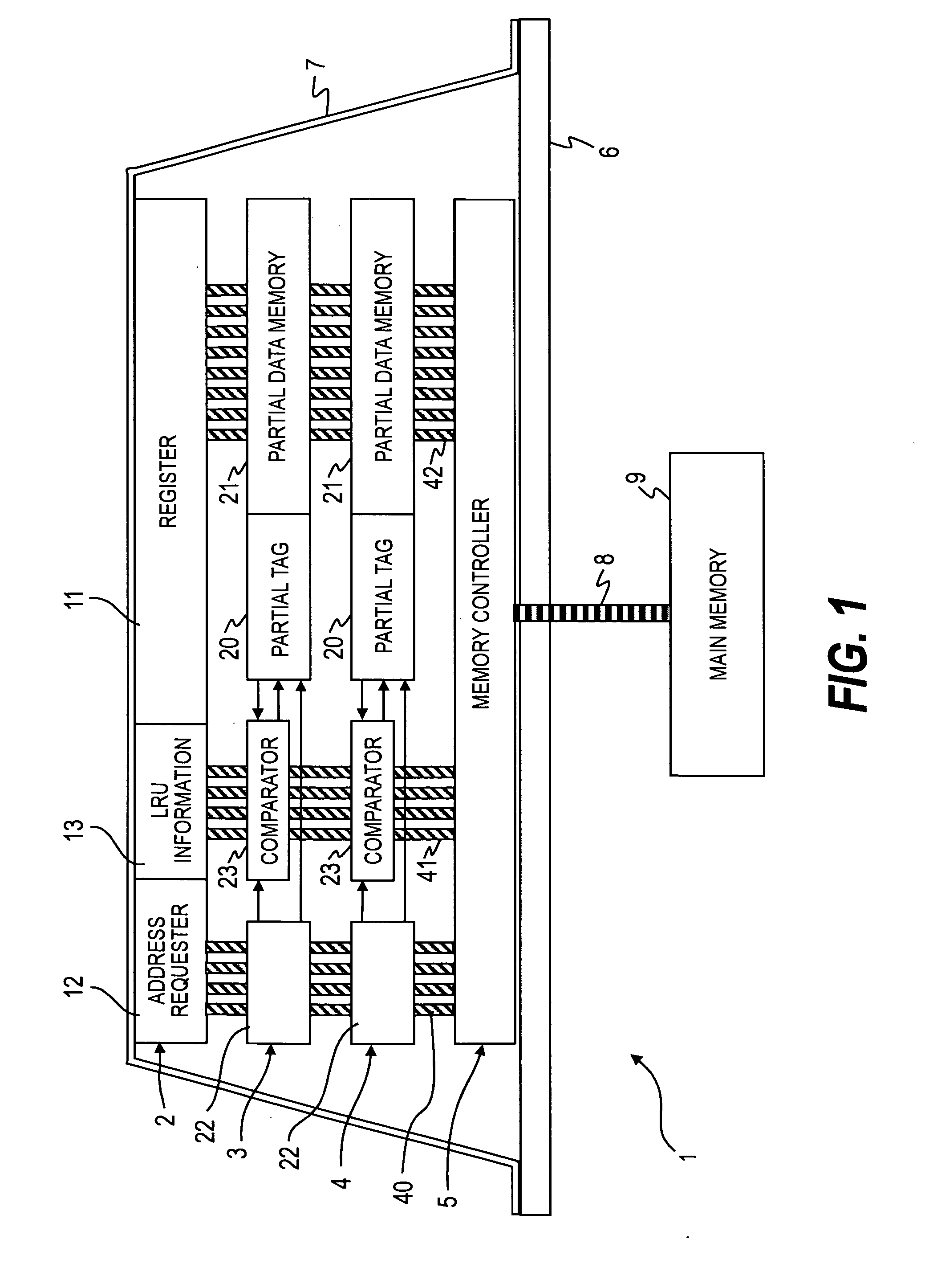
[0068]FIG. 5 is a sectional view showing important parts of the processor 1 according to a second embodiment of this invention. The second embodiment is obtained by modifying the LRU information storing unit 13 of the first embodiment. The CPU-LSI 2 of the second embodiment has, in place of the LRU information storing unit 13 of the first embodiment, a chip LRU information storing unit 13A which keeps chip LRU information for identifying which of the cache LSI-A and the cache LSI-B is available for refilling. The cache LSI-A and the cache LSI-B each have a partial LRU information storing unit 130 which keeps partial LRU information for identifying which cache line in the cache LSI is available for refilling. The rest of the second embodiment is the same as the first embodiment.

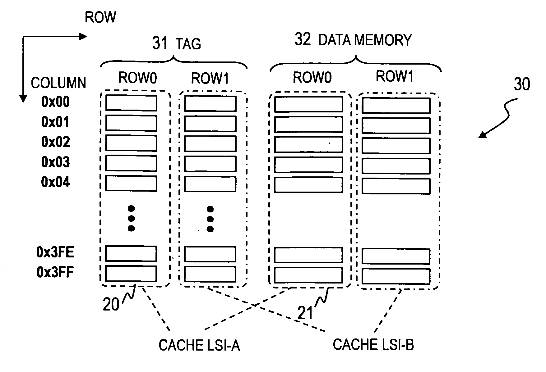
[0069]The LRU information, which is small in capacity compared to tags as mentioned above, still takes up a fair capacity when the cache LSI-A and the cache LSI-B have many cache lines. To reduce the capacity ...

third embodiment

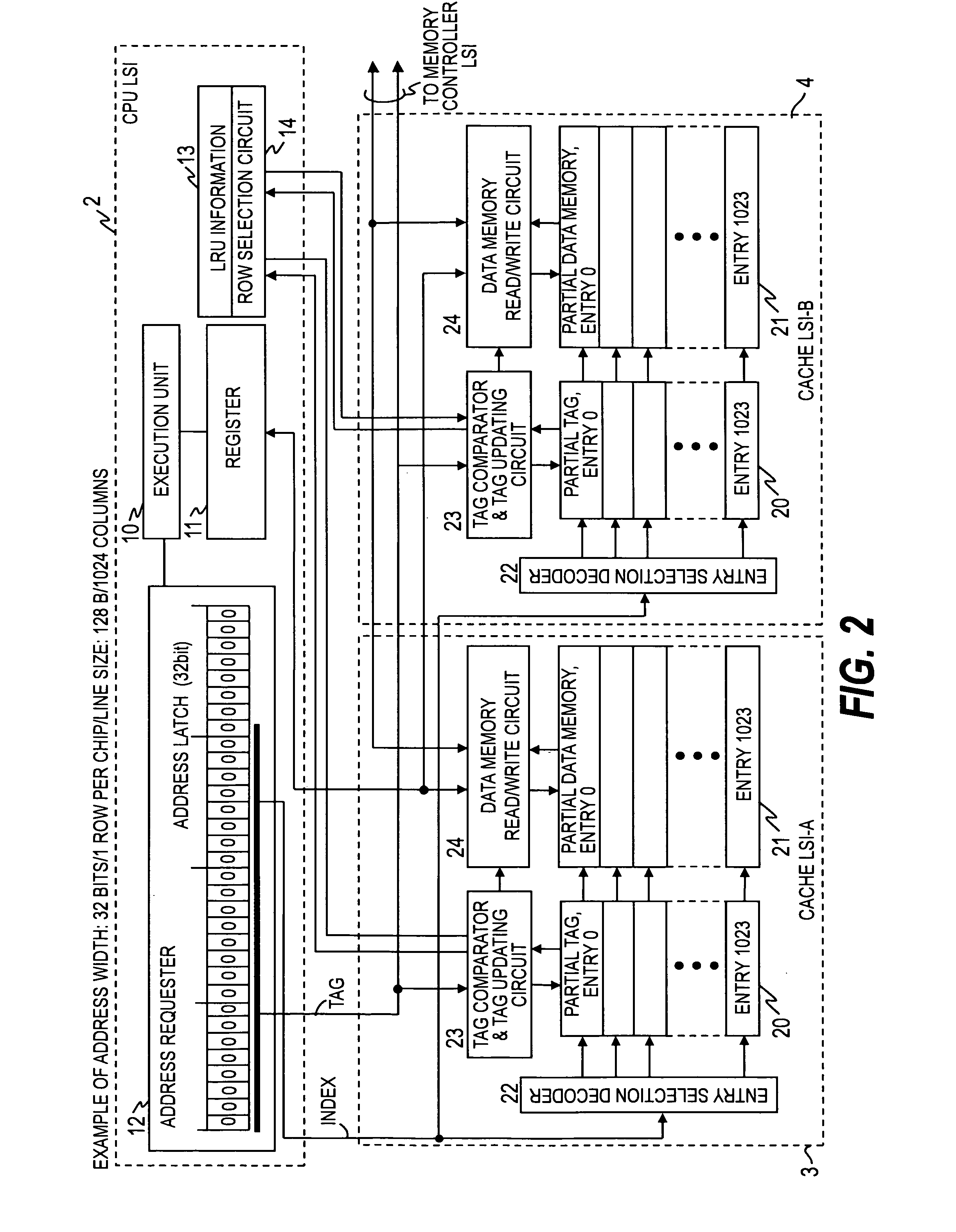
[0072]FIG. 6 is a sectional view showing important parts of the processor 1 according to a third embodiment of this invention. In the third embodiment, the through electrode 40 of the first embodiment is changed from parallel signal lines to serial signal lines, and a serial-parallel conversion circuit is added to each LSI to transfer bit string information. The address requester 12 of the CPU-LSI 2 is provided with a parallel-serial conversion circuit (serializer (SER) circuit) 120, which sends address information to a through electrode 40A formed of serial signal lines, the entry selection decoders 22 of the cache LSI-A and the cache LSI-B are each provided with a serial-parallel conversion circuit (deserializer (DES) circuit) 220, which converts serial signals of the through electrode 40A into parallel signals, and the memory controller LSI 5 is provided with a serial-parallel conversion circuit (DES circuit) 520. The rest of the third embodiment is the same as the first embodime...

fourth embodiment

[0074]FIGS. 7 and 8 show a fourth embodiment of this invention, and an application of SIP packaging in which the LSIs of the first embodiment are linked by a plate-like interposer 60. The structures of the LSIs 2 to 5 are the same as those in the first embodiment.

[0075]FIG. 7 is a plan view showing important parts of a processor 1A on the interposer 60. FIG. 8 is a sectional view of the processor 1A.

[0076]In FIG. 7, the LSIs are placed on the interposer 60 such that the CPU-LSI 2, the cache LSI-A, the cache LSI-B, and the memory controller LSI 5 are arranged in the stated order from top to bottom of the drawing. The LSIs 2 to 5 are disposed on the top surface of the plate-like interposer 60 as shown in FIG. 8.

[0077]Wiring lines laid on the interposer 60 replace the through electrodes of the first embodiment. Wiring 640 is used to broadcast address information from the address requester 12 to the cache LSI-A, the cache LSI-B, and the memory controller LSI 5. Wiring 641 is used to bro...


PUM


Abstract

To provide an easy way to constitute a processor from a plurality of LSIs, the processor includes: a first LSI containing a processor; a second LSI having a cache memory; and information transmission paths connecting the first LSI to a plurality of the second LSIs, in which the first LSI contains an address information issuing unit which broadcasts, to the second LSIs, via the information transmission paths, address information of data, the second LSI includes: a partial address information storing unit which stores a part of address information; a partial data storing unit which stores data that is associated with the address information; and a comparison unit which compares the address information broadcast with the address information stored in the partial address information storing unit to judge whether a cache hit occurs, and the comparison units of the plurality of the second LSIs are connected to the information transmission paths.

Description

CLAIM OF PRIORITY[0001]The present application claims priority from Japanese application P2007-337083 filed on Dec. 27, 2007, the content of which is hereby incorporated by reference into this application.BACKGROUND OF THE INVENTION[0002]This invention relates to a structure of a cache memory of a processor, and more particularly, to a technique of cache memory construction that includes stacking a plurality of large scale integrations (LSI).[0003]Device miniaturization owing to the recent advancement in semiconductor manufacture technology has made it possible to integrate numerous transistors on one die, and now a few or many processor cores can be integrated on one die or in one package. Multi-core processors having a plurality of processor cores, for example, have an exponentially improved computing ability.[0004]Meanwhile, the transfer rate of DRAMs widely employed as a main memory which stores data read and written by a processor has not kept up with the aforementioned improve...

Claims


Application Information

Patent Timeline
IPC IPC(8): G06F12/08
CPCG06F2212/1056G06F2212/1048G06F12/0893G06F12/0864
Inventor SUKEGAWA, NAONOBU
Owner HITACHI LTD
Learn More