Clock synchronization circuit and operation method thereof

a clock synchronization and circuit technology, applied in the field of semiconductor design technology, can solve the problems of jitter, which is mixed with the external clock signal and inputted to the internal circuit, cannot be ignored in high frequency operation, and the jitter peak phenomenon seriously worsens the jitter of the pll clock signal clk_pll, so as to improve the operating characteristics of jitter, stable phase/frequency locking operation and power consumption

Inactive Publication Date: 2009-07-09
SK HYNIX INC
View PDF3 Cites 68 Cited by
  • Summary
  • Abstract
  • Description
  • Claims
  • Application Information

AI Technical Summary

Benefits of technology

[0034]Since the clock synchronization circuit according to the invention operates based on an open-loop system, the jitter peaking phenomenon does not occur. Also, since a filtered control voltage is used, no pattern jitter of the oscillation control voltage signal occurs in generating the internal clock signals. Meanwhile, the clock synchronization circuit according to the invention can improve the operating characteristics of the jitter with a stable phase / frequency locking operation as well as power consumption.

Problems solved by technology

Jitter, which is mixed with the external clock signal and inputted to the internal circuit, cannot be disregarded in high frequency operation.
This jitter peaking phenomenon seriously worsens the jitter of the PLL clock signal CLK_PLL by amplifying jitter caused by power noise as well as the input jitter.
The reason that the jitter peaking phenomenon is caused is that the phase-locked loop, which is a closed-loop system having two poles in the frequency domain (s-domain), does not secure a desired phase margin in the phase / frequency locking process.
For example, the response time may be fast when the phase margin of such a system is smaller than 60°; however, it will take the signal a lot of time to come back to the steady state because of the high instability of the signal.
On the contrary, if the phase margin of the system is larger than 60°, the stability can be improved; however, the response time is slow so that it will take the signal a lot of time to come back to the steady state.
However, for the following reasons it is still difficult to design a phase-locked loop which has a desired phase margin.
Therefore, since the phase margin is small and the jitter peaking phenomenon occurs, the signal jitter included in the signal is amplified and the power noise also largely amplifies the jitter.
As a result, the PLL clock signal CLK_PLL deteriorates seriously.
However, there is another problem in that the pattern jitter, which is periodically generated, is increased because of the ripple of the oscillation control voltage signal V_CTR.
That is, in the phase-locked loop, there is a problem that the pattern jitter of the oscillation control voltage signal V_CTR is largely caused when the resistance value of the resistor R is increased to remove the jitter peaking phenomenon, and there is another problem that the jitter peaking phenomenon is also caused when the resistance value of the resistor R is decreased to remove the pattern jitter.
However, a preferred filtering operation cannot be achieved because of the jitter peaking phenomenon in the jitter transfer function of the phase-locked loop.
Further, if the resistance value of the resistor R is adjusted in order to remove the jitter peaking phenomenon, the pattern jitter of the oscillation control voltage signal V_CTR is increased so that an exact phase / frequency locking operation cannot be achieved.

Method used


Image

  • Clock synchronization circuit and operation method thereof
  • Clock synchronization circuit and operation method thereof
  • Clock synchronization circuit and operation method thereof

Examples


Embodiment Construction

[0050]Hereinafter, the present invention will be described in detail with reference to several embodiments. The embodiments merely exemplify the invention, and the scope of invention rights to be protected is not limited thereby.

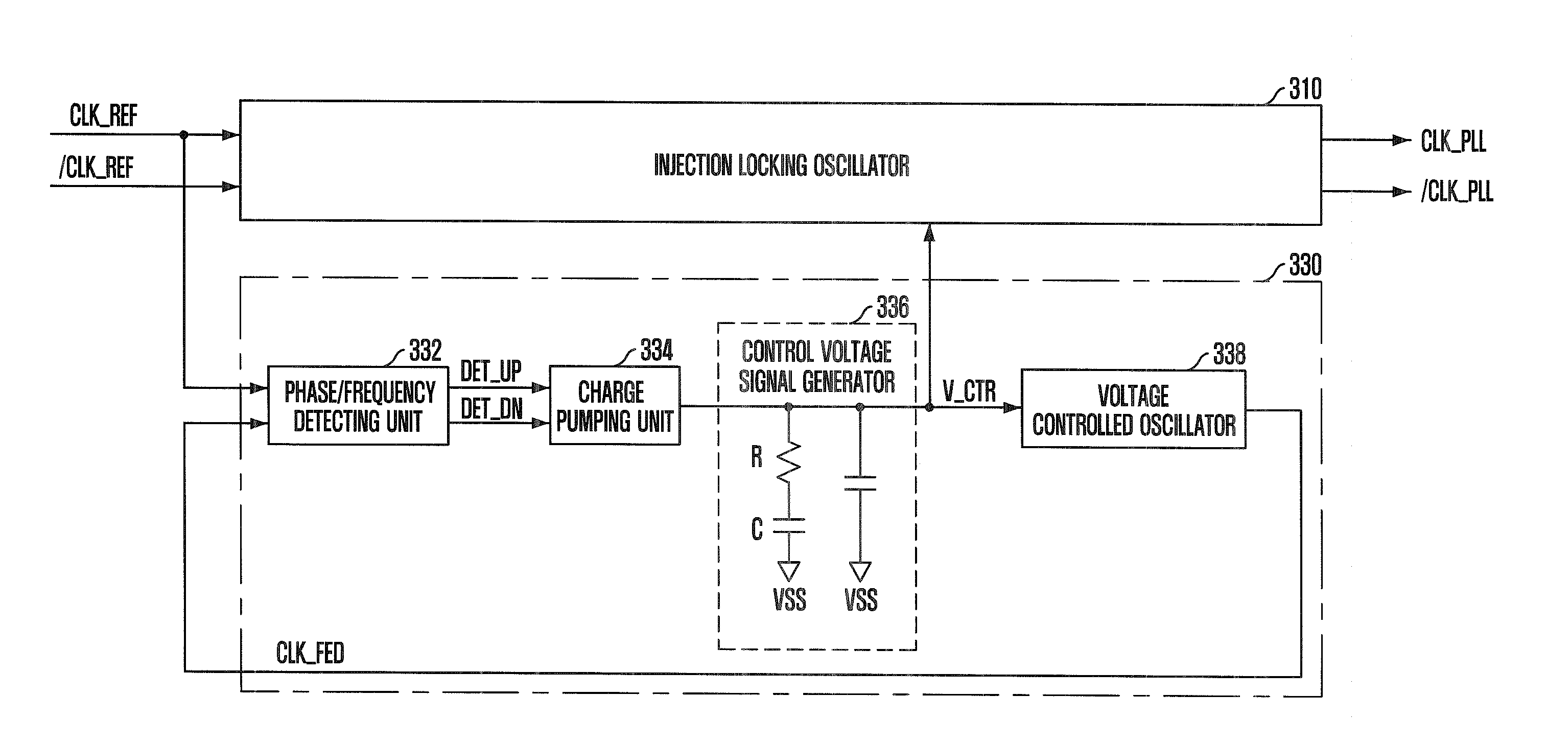
[0051]FIG. 3 is a block diagram illustrating a clock synchronization circuit according to the invention. Referring to FIG. 3, the clock synchronization circuit includes an injection locking oscillator 310 and a phase-locked loop 330.

[0052]In the injection locking oscillator 310, a free running frequency is set up in response to an oscillation control voltage signal V_CTR which is generated by the phase-locked loop 330, and PLL clock signals CLK_PLL and / CLK_PLL are generated in synchronization with reference clock signals CLK_REF and / CLK_REF. The detailed circuit and operation are described below. For reference, the reference clock signals CLK_REF and / CLK_REF correspond to an external clock signal. The positive reference clock signal CLK_REF is generated i...


PUM


Abstract

A semiconductor memory device with a clock synchronization circuit capable of performing a desired phase/frequency locking operation, without the jitter peaking phenomenon and the pattern jitter of an oscillation control voltage signal using injection locking. The device includes a phase-locked loop that detects a phase/frequency difference between a feedback clock signal and a reference clock signal to generate an oscillation control voltage signal corresponding to the detected phase/frequency difference, and generates the feedback clock signal corresponding to the oscillation control voltage signal. An injection locking oscillation unit sets up a free running frequency in response to the oscillation control voltage signal and generates an internal clock signal which is synchronized with the reference clock signal.

Description

CROSS-REFERENCE TO RELATED APPLICATIONS[0001]The present invention claims priority of Korean patent application numbers 10-2008-0002042 and 10-2008-0030293, filed on Jan. 8, 2008 and Apr. 1, 2008, respectively, which are incorporated by reference in their entirety.BACKGROUND OF THE INVENTION[0002]The present invention relates to a semiconductor design technology and, more particularly to a clock synchronization circuit and a method for operating the same.[0003]Generally, in a semiconductor memory device including a DDR SDRAM (Double Data Rate Synchronous DRAM), internal clock signals are produced using an external clock signal and these internal clock signals are used as reference clock signals for synchronization with various operation timing. Accordingly, a clock synchronization circuit for synchronizing the external clock signal and the internal clock signals is provided in the semiconductor memory device. A typical clock synchronization circuit is a phase-locked loop (PLL).[0004...

Claims


Application Information

Patent Timeline
Patent Type & Authority Applications(United States)
IPC IPC(8): G11C8/18H03L7/06
CPCG11C7/22G11C7/222G11C8/18H03K2005/00208H03L7/24H03L7/083H03L7/0891H03L7/0995H03L7/0805
Inventor SONG, TAEK-SANGKIM, KYUNG-HOONKWON, DAE-HANYOON, DAE-KUM
Owner SK HYNIX INC
Why Eureka
Try Eureka