Nano/micro-textured surfaces and methods of making same by aluminum-induced crystallization of amorphous silicon

a nano- and micro-scale technology, applied in the direction of vacuum evaporation coating, chemical vapor deposition coating, eyeglasses, etc., can solve the problems of safety issues, endoscopic lenses and dentist's mirrors can be fogged, and vehicle windows and lenses of eyeglasses can become foggy, so as to promote cell growth and enhance cell attachment to a surface

Inactive Publication Date: 2009-07-09
ZOU MIN +1
View PDF3 Cites 120 Cited by
  • Summary
  • Abstract
  • Description
  • Claims
  • Application Information

AI Technical Summary

Benefits of technology

[0010]The present invention relates to a method of surface texturing at nano- and micro-scale by aluminum-induced rapid crystallization (AIRC) of am

Problems solved by technology

In winters, window-glasses of vehicles and lenses of eyeglasses can become foggy because the water vapor in air condenses on these surfaces.
Similarly, endoscopic lenses and the mirrors used by dentists can be fogged by the condensation of the hot moisture in patients on the cold surfaces.
Foggy surfaces can create safety is

Method used


Image

  • Nano/micro-textured surfaces and methods of making same by aluminum-induced crystallization of amorphous silicon
  • Nano/micro-textured surfaces and methods of making same by aluminum-induced crystallization of amorphous silicon
  • Nano/micro-textured surfaces and methods of making same by aluminum-induced crystallization of amorphous silicon

Examples


first embodiment

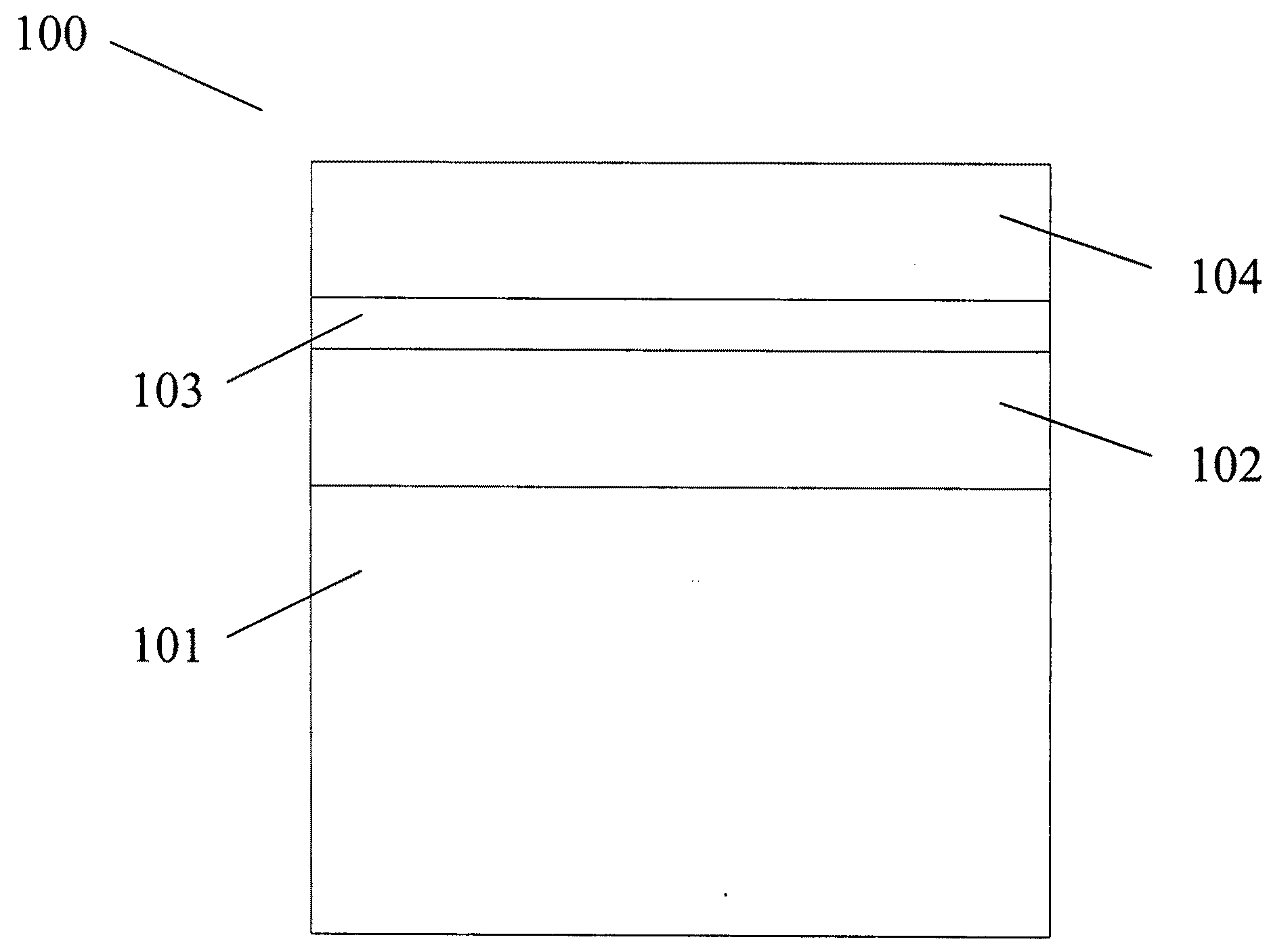
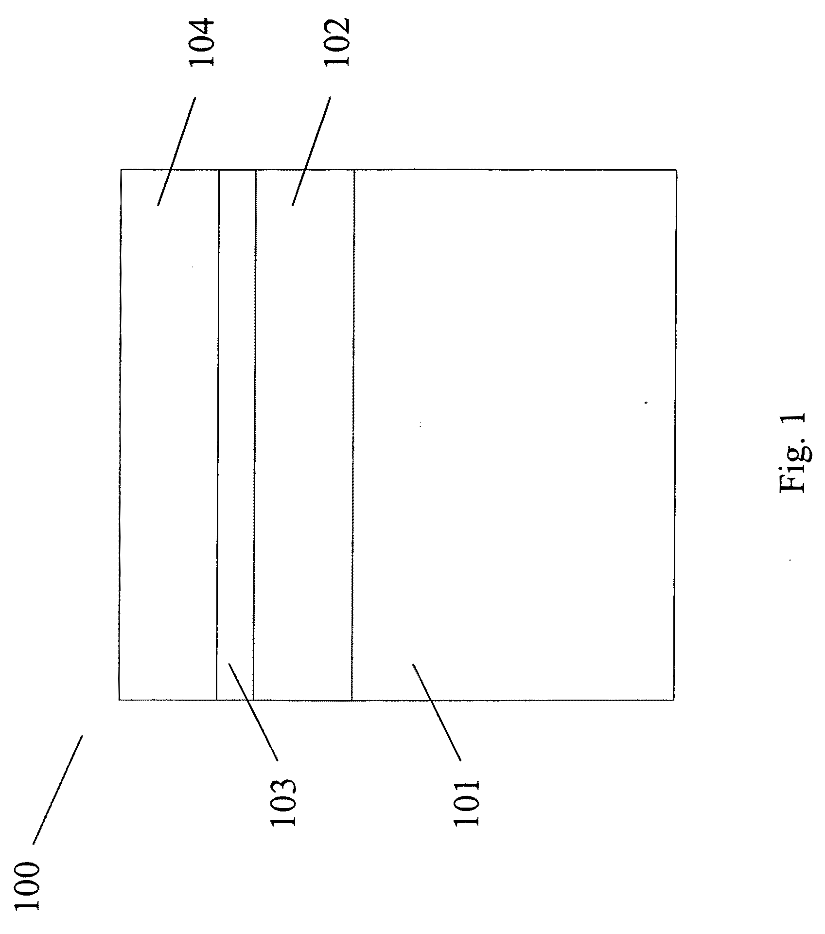
[0037]Referring to FIG. 1, a plasma-enhanced chemical vapor deposition (PECVD) system is used to deposit a layer of a-Si 102 on a silicon oxide coated silicon (100) wafer 101 to form a sample. After the deposition of a-Si 102, the sample is removed from the PECVD system and exposed to air to form a thin layer of native oxide 103 on top of the a-Si 102. The sample is then transferred to an evaporator for thermal deposition of a layer of Al 104 on top of the native silicon oxide 103 to form a multi-layer structure 100. The structure 100 is annealed in air in a conventional furnace. After annealing, the excessive Al on structure 100 is removed by wet selective etching, resulting in nano / micro-textured surfaces.

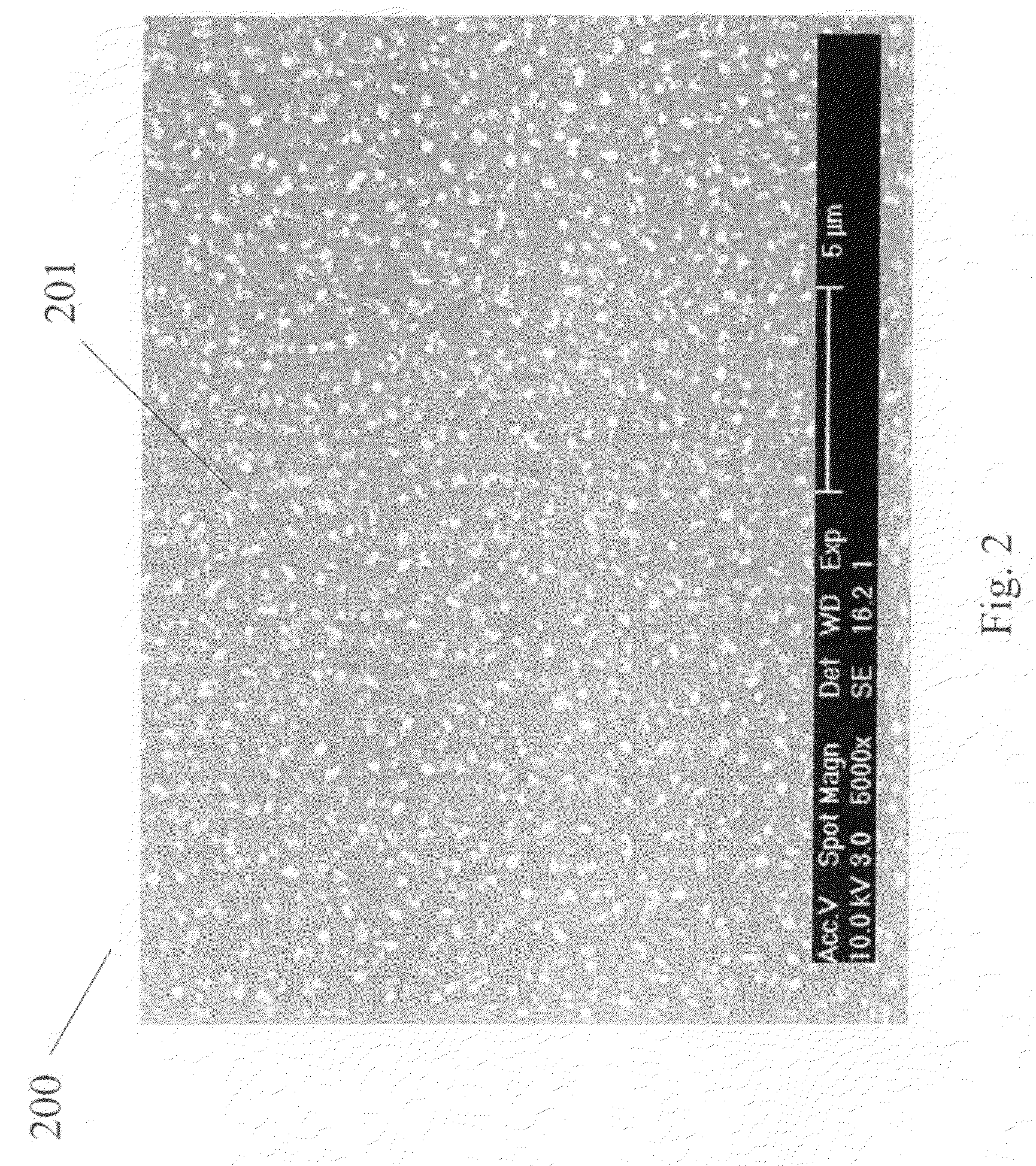
[0038]FIG. 2 shows an SEM image of a textured surface 200 produced by the method illustrated in FIG. 1. The bright spots 201 are randomly distributed nano- / micro-silicon crystallites. FIG. 3 is an EDS spectrum taken from the textured surface 200. The spectrum 300 contains a large...

second embodiment

[0039]Referring to FIG. 6, a thermal evaporator is used to deposit a layer of Al 602 on a silicon oxide coated silicon (100) wafer 601 to form a sample. After the deposition of Al 602, the sample is removed from the evaporator and exposed to air to form a thin layer of aluminum oxide 603 on top of the Al 602. The sample is then transferred to a PECVD system for the deposition of a layer of a-Si 604 on top of the aluminum oxide 603 to form a multi-layer structure 600. The structure 600 is annealed in air in a conventional furnace. During annealing, some Al diffuses through the a-Si layer 604 to the top surface of the sample 600. After annealing, the Al that passed through the a-Si 604 is removed by wet selective etching, resulting in nano / micro-textured surfaces.

third embodiment

[0040]Referring to FIG. 7, using an e-beam evaporator, a layer of a-Si and Al mixture 702 is deposited on a silicon oxide coated silicon (100) wafer 701 to form a sample 700. The sample 700 is annealed in air in a conventional furnace. During annealing, some Al diffuses to the top surface of the sample 700. After annealing, the excessive Al on the top surface of the structure 700 is removed by wet selective etching, resulting in nano / micro-textured surfaces.

[0041]In the following examples, various process parameters will be described to illustrate how to use the technique to control the surface wettability and promote cell attachment on a surface in detail. These examples are for illustration purpose only. These specific materials, parameters, and equipment used in the examples are not meant to limit the scope of the invention.


PUM

PropertyMeasurementUnit
Thicknessaaaaaaaaaa
Wettabilityaaaaaaaaaa
Superhydrophobicityaaaaaaaaaa

Abstract

The present invention discloses a method of surface texturing at nano/micro-scale by aluminum-induced rapid crystallization of amorphous silicon for controlling the wettability of a surface, enhancing cell attachment to a surface, and promoting cell growth on a surface. The present invention can be used in a variety of applications, such as producing superhydrophobic or superhydrophilic surfaces for medical devices, microelectromechanical systems, and microfluidic channels.

Description

CROSS-REFERENCE TO RELATED PATENT APPLICATION[0001]This application claim priority to U.S. Provisional Patent Application Ser. No. 61 / 020,014, filed Jan. 9, 2008, entitled “NANO / MICRO-TEXTURED SURFACES AND METHODS OF MAKING SAME BY ALUMINUM-INDUCED CRYSTALLIZATION OF AMORPHOUS SILICON” by Min Zou and Hengyu Wang.FIELD OF THE INVENTION[0002]The present invention relates primarily to a method of surface texturing and its applications, and more specifically, to a method of surface texturing at nano- / micro-scale by aluminum-induced rapid crystallization of amorphous silicon for uses in controlling surface wetting properties, promoting cell attachment on a surface, and promoting cell growth on a surface.BACKGROUND OF THE INVENTION[0003]Surface textures have wide applications: they can be used to control the wetting properties of a surface and to promote cell attachment and growth on a surface [1-4].[0004]Superhydrophobicity and superhydrophilicity are two valuable wetting properties of a...

Claims


Application Information

Patent Timeline
IPC IPC(8): B05D5/02
CPCC23C14/18C23C16/56C23C16/24C23C14/5806
Inventor ZOU, MINWANG, HENGYU
Owner ZOU MIN
Why Eureka
Try Eureka