Memory bus shared system

a memory bus and shared technology, applied in the direction of memory adressing/allocation/relocation, generating/distributing signals, instruments, etc., can solve the problem of affecting the operation of the dvd driver, and achieve the effect of reducing the pin terminal number of the controller, increasing the data transfer rate, and reducing the number of bus utilization efficiency

Active Publication Date: 2009-07-09
TEXAS INSTR INC
View PDF3 Cites 14 Cited by
  • Summary
  • Abstract
  • Description
  • Claims
  • Application Information

AI Technical Summary

Benefits of technology

[0009]In the aforementioned constitution, since the address terminals and data terminals of the controller are shared in address assignment and data transfer with respect to the first and second memories, the pin terminal number of the controller can be reduced significantly. Also, by performing alternate operation without competition or conflict on the same address bus or data bus for the first memory in synchronization with a clock and the asynchronous second memory independent of a clock, it is possible to improve both the data transfer efficiency (bus utilization efficiency) and the data transfer efficiency.
[0010]As a preferable embodiment of the present invention, said first memory, said second memory and said controller are carried on individual semiconductor chips, respectively, and are assembled on the same substrate or in a package. In this case, since the controller can be made of a semiconductor package with a lower pin number, it is possible to cut the substrate cost and the assembly cost.
[0019]In the aforementioned constitution, the address terminals of the controller are shared in address assignment with respect to the first and second memories, so that it is possible to reduce the pin terminal number of the controller. Here, the first memory in synchronization with a clock and the asynchronous second memory independent of a clock are in operation alternately without competition or conflict on the same address bus. As a result, it is possible to improve the data transfer efficiency (bus utilization efficiency) and the data transfer rate.
[0021]In the aforementioned constitution, since the address terminals of the controller are shared in address assignment and data transfer with respect to the synchronous DRAM and flash memory, it is possible to significantly reduce the pin terminal number of the controller. Here, the synchronous DRAM in synchronization with a clock and the asynchronous flash memory independent of a clock are in operation alternately without competition or collision on the same address bus and data bus. Also, even if the burst length of the synchronous DRAM is large, it is possible to execute burst transfer in plural rounds with data access of the flash memory sandwiched between them. As a result, it is possible to further increase the data transfer efficiency (bus utilization efficiency) and the data transfer rate.

Problems solved by technology

As a result, as the DFE package becomes larger, the substrate size becomes larger, and this leads to a larger size of the DVD driver.

Method used


Image

  • Memory bus shared system
  • Memory bus shared system
  • Memory bus shared system

Examples


embodiment 1

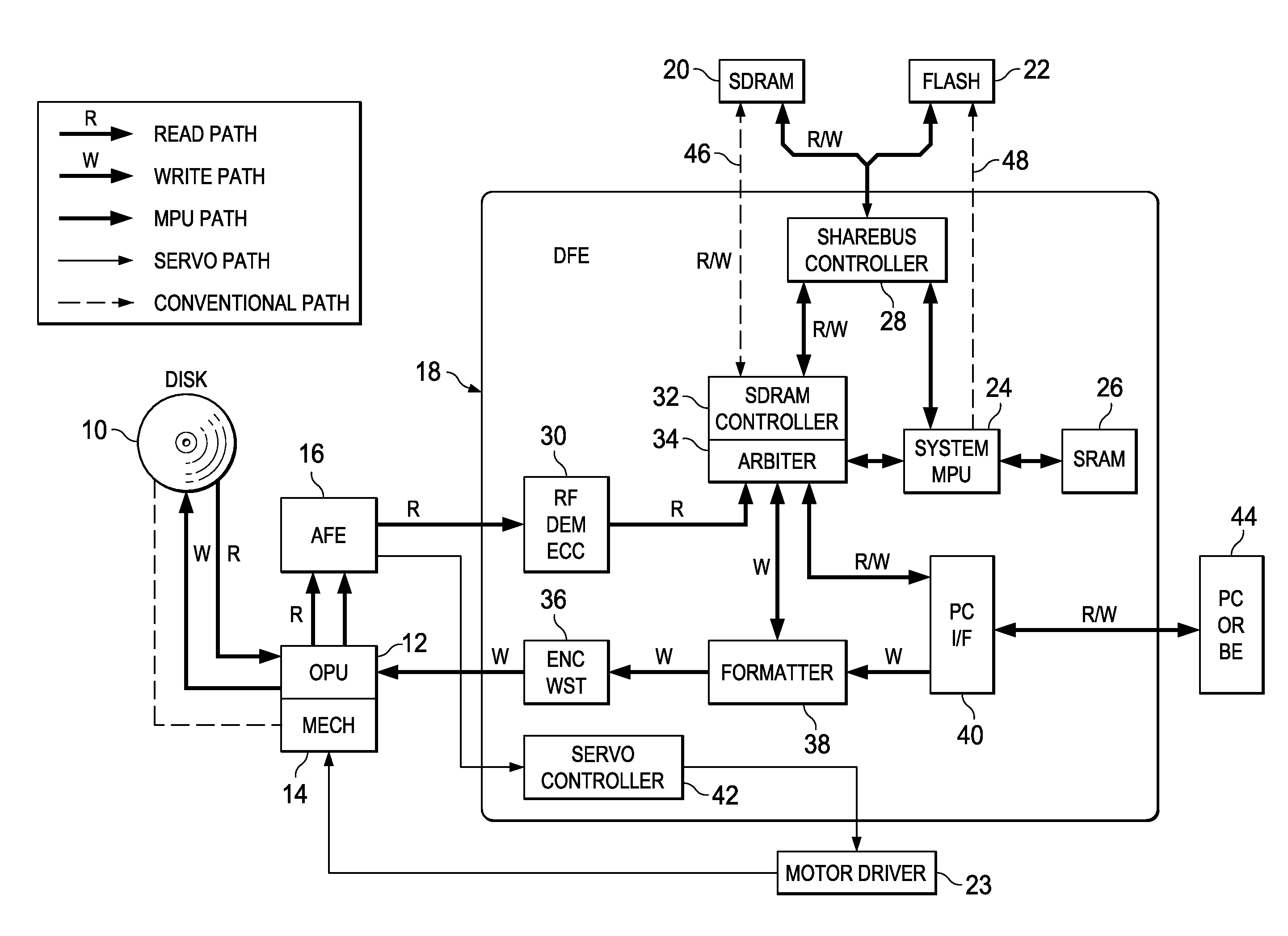
[0053]FIG. 4 is a diagram illustrating the state of connection between DFE 18 and SDRAM 20, FLASH 22 in the embodiment (Embodiment 1). FIG. 6 is a diagram illustrating the detailed pin configuration of said semiconductor packages 18, 20, 22 and an example of layout of the printed wiring. In FIG. 6, the printed board (not shown in the figure) having said semiconductor packages 18, 20, 22 assembled on it is made of a laminated wiring board containing wiring groups (50A), (50B), (50C), (50D) as a first layer of wiring, and wiring groups (52A), (52B), (52C) as a second layer of wiring.

[0054]As shown in FIG. 4, for DFE 18, MCLK represents a system clock output terminal, and MCKE represents a clock enable output terminal. They are respectively connected via individual control lines to clock input terminal CLK and clock enable input terminal CKE of SDRAM 20.

[0055]For DFE 18, MRAS represents a row address strobe output terminal, MCAS represents a column address strobe output terminal, and M...

embodiment 2

[0091]In Embodiment 2 shown in FIG. 12, the data of FLASH 22 have an 8-bit configuration, and the address has a 21-bit configuration. More specifically, data terminals D [15:0] of 16 bits of SDRAM 20 are connected to MD terminals [15:0] of 16 bits of DFE 18 via data bus D-Bus 1 with a width of 16 bits, and the 10-bit address terminals A [9:0] of SDRAM 20 are connected to 10-bit address terminals MA [9:0] of DFE 18 via 10-bit-width address bus A-Bus 1. Also, the 21-bit address terminals A [20:0] of FLASH 22 are connected via 10-bit address bus A-Bus 2 and 11-bit address bus A-Bus 3 to 10-bit address terminals CA [9:0] and 11-bit address terminals CA [20:10] of DFE 18. Here, In DFE 18, address terminals CA [9:0] and address terminals MA [9:0] are Identical to each other. Also, the 8-bit data terminals DQ [7:0] of FLASH 22 are connected to 8-bit data terminals CD [7:0] of DFE 18 via 8-bit data bus D-Bus 2.

[0092]As explained above, in this Embodiment 2, a portion [9:0] of address termin...

embodiment 3

[0094]Also in said Embodiment 3, a portion [9:0] of address terminals A [19:0] of DFE 18 is connected commonly to address bus A-Bus 1 on the side of SDRAM 20 and address bus A-Bus 2 on the side FLASH 22. By means of this address bus sharing scheme, for SDRAM 20 with 35 pins and FLASH 22 with 32 pins, DFE 18 has 64 pins for allotting to two memories 20, 22.

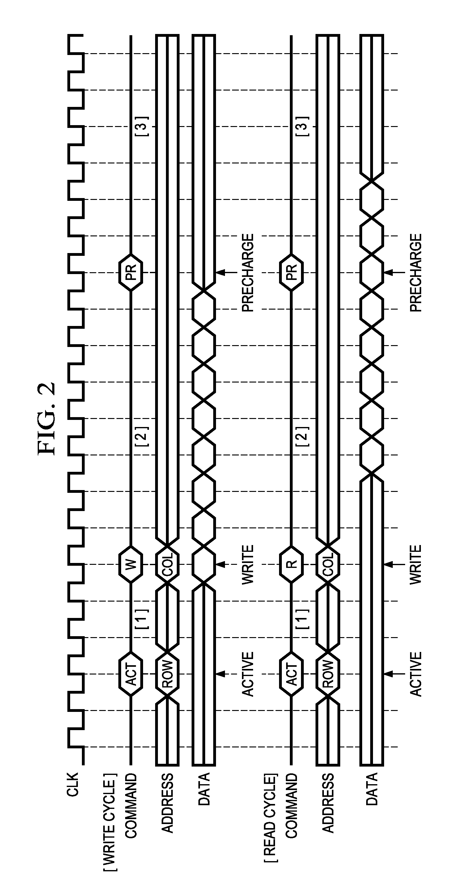
[0095]FIGS. 14 and 15 are timing diagrams illustrating the protocol for avoiding competition between access of SDRAM 20 and access of FLASH 22 in the bus shared system in Embodiments 2 and 3. FIG. 14 is a diagram illustrating write access as the access of SDRAM 20, and read access as the access to FLASH 22. As shown in FIG. 15, the access to SDRAM 20 is read access, and the access to FLASH 22 is the read access.

[0096]As shown in the figures, from before the end of transfer of the write data (#1 . . . #N) on the side of SDRAM 20 on data bus D-Bus 1, it is possible to output the data read to data bus D-Bus 2 from FLASH 22. As a resul...


PUM


Abstract

The invention reduces the pin terminal number of a controller that in parallel or simultaneously accesses a synchronous memory and an asynchronous memory. When a column address is latched to an SDRAM, immediately after that, access to FLASH is started, and a shared bus controller outputs the write / read address with respect to FLASH on the address bus. Then, after the end of data transfer on the data bus, either the shared bus controller outputs the write data, or FLASH can output the read data on the data bus by means of a strobe signal. Then, the input of address is established by FLASH, and, as the shared bus controller asserts a strobe signal, either FLASH fetches the write data on the data bus, or the shared bus controller fetches the read data on the data bus.

Description

FIELD OF THE INVENTION[0001]The present invention pertains to a type of memory system for signal processing and data processing. Especially, the present invention pertains to a type of memory bus shared system that shares a bus for different types of memories.BACKGROUND OF THE INVENTION[0002]Usually, in digital signal processing, a semiconductor memory is used together with a microprocessor. There are two types of semiconductor memories, that is, a volatile memory and a nonvolatile memory. When both types are used together in a single system, the volatile memory is mainly used for temporary storage of data, while the nonvolatile memory is mainly used for storage of programs and fixed values.[0003]In recent years, with improvement in the processability of microprocessors (MRU), a higher rate is required for the volatile memory, and a large capacity is required for the nonvolatile memory. The main type of high rate volatile memory is a synchronous DRAM (SDRAM), and the main type of la...

Claims


Application Information

Patent Timeline
Patent Type & Authority Applications(United States)
IPC IPC(8): G06F1/12G06F13/00G06F12/00G06F12/02
CPCG06F3/0626G06F13/1694G06F3/0679G06F3/0658
Inventor TAHARA, MASAYUKI
Owner TEXAS INSTR INC
Why Eureka
Try Eureka