Method for forming gate oxide of semiconductor device

a gate oxide and semiconductor technology, applied in semiconductor devices, semiconductor/solid-state device details, electrical devices, etc., can solve the problems of reducing production yield, difficult to secure a margin for a patterning process using photoresist, increasing manufacturing cost and time, etc., to improve the threshold voltage characteristic, improve the characteristics and uniformity of the gate oxide, and improve the level of the interface trap charge (dit) level and threshold voltage. , the effect of enhancing the reliability of the semiconductor devi

Active Publication Date: 2009-07-16
KEY FOUNDRY CO LTD
View PDF2 Cites 9 Cited by
  • Summary
  • Abstract
  • Description
  • Claims
  • Application Information

AI Technical Summary

Benefits of technology

[0018]The present invention can form a gate oxide having a triple structure of a wet oxide film/TEOS oxide film/nitride film in a high voltage region and harden the TEOS oxide film when a gate oxide of a medium voltage region is formed to improve characteristics and uniformity of the g

Problems solved by technology

This increases the manufacturing cost and time and decreases production yield.
Furthermore, it is difficult to secure a margin for a patterning process using photoresist as the integration of the semiconductor device increases.
Moreover, a cleaning process is required to selectively remove the oxide films to cause generation

Method used


Image

  • Method for forming gate oxide of semiconductor device
  • Method for forming gate oxide of semiconductor device
  • Method for forming gate oxide of semiconductor device

Examples


Embodiment Construction

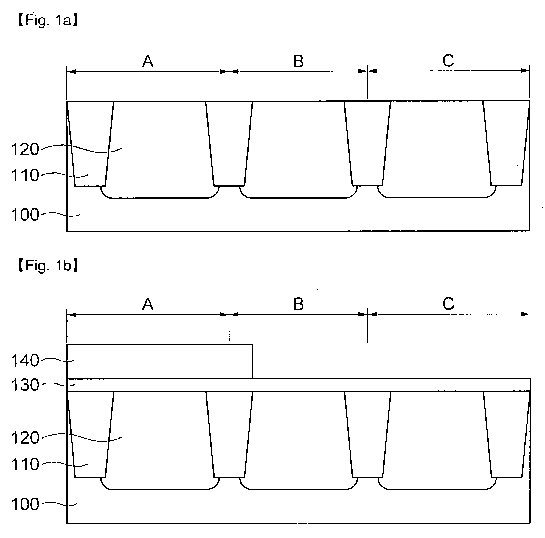
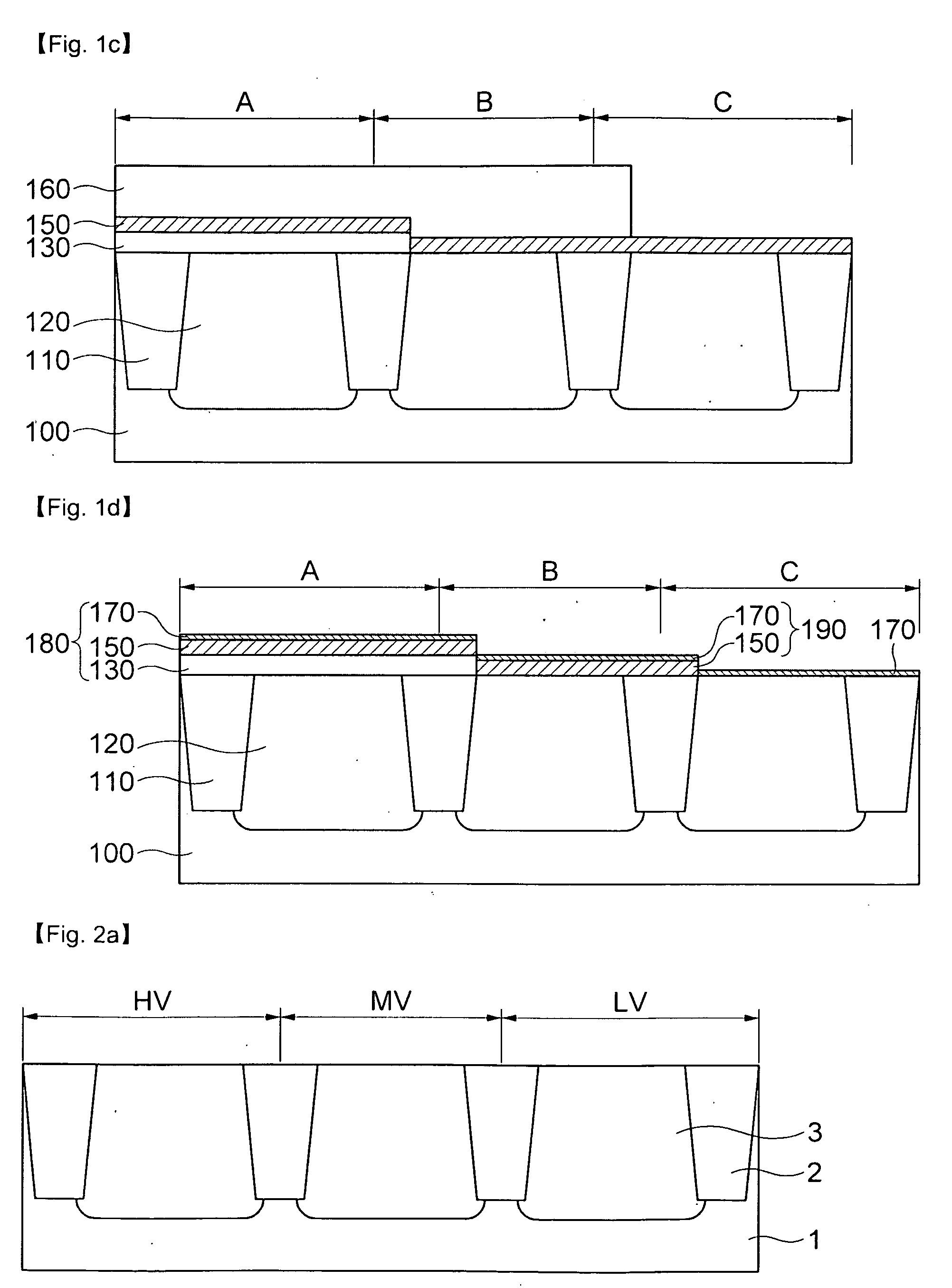
[0024]FIGS. 2a through 2h are cross-sectional views illustrating a method for forming a gate oxide of a semiconductor device according to an embodiment of the present invention.

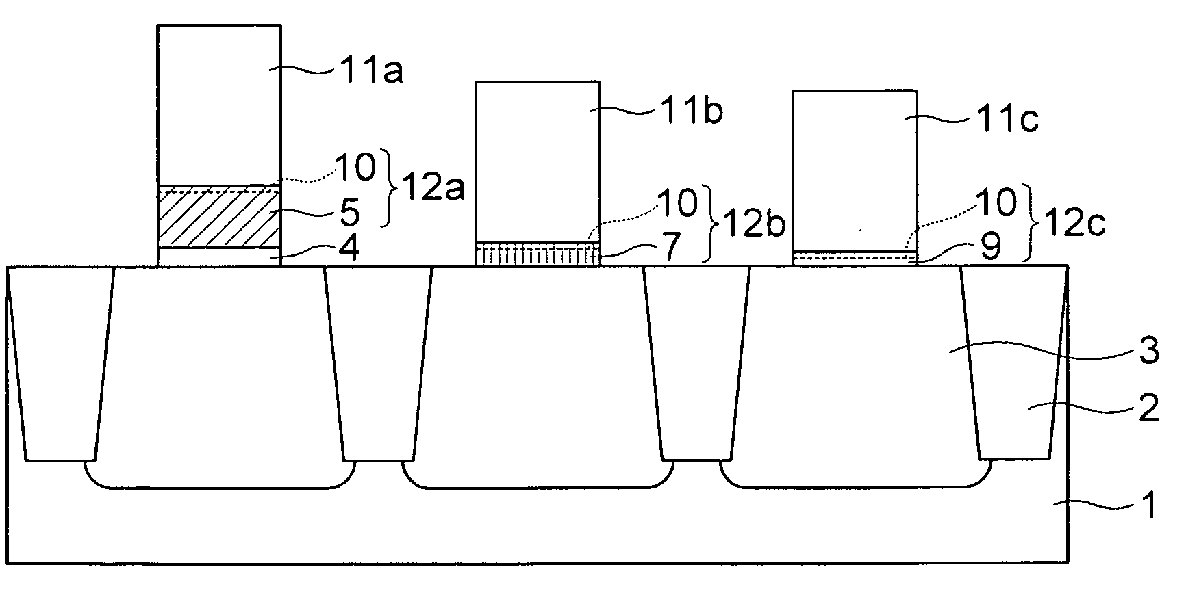
[0025]Referring to FIG. 2a, an isolation layer 2 is formed in a semiconductor substrate 1 to define a high voltage region HV, a medium voltage region MV and a low voltage region LV. Ion implantation is performed to respectively form wells 3 in the high voltage region HV, the medium voltage region MV and the low voltage region LV.

[0026]Referring to FIG. 2b, a first oxide film 4 is formed by a predetermined thickness on the overall surface of the semiconductor substrate 1 and a second oxide film 5 is formed thereon. Here, the first oxide film 4 is formed in order to improve interface trap charge (Dit) characteristic of Si / SiO2 interface.

[0027]The first oxide film 4 is formed of a wet oxide in the ambient of H2 / O2 by a thickness in the range of 40 to 220 Å at a temperature in the range of 800 to 900° C. and the ...


PUM


Abstract

The method for forming a triple gate oxide of a semiconductor device includes the steps of defining a first region, a second region and a third region, forming a first oxide film and forming a second oxide film on the first oxide film, blocking the first region and selectively removing portions the second oxide film and the first oxide film, forming a third oxide film on the semiconductor substrate, blocking the first region and the second region and selectively removing a portion of the third oxide film and forming a fourth oxide film on the semiconductor substrate and then forming a nitride film thereon, wherein a gate oxide having a triple structure is formed in the first region, a gate oxide having a double structure is formed in the second region and a gate oxide having a double structure is formed in the third region.

Description

BACKGROUND OF THE INVENTION[0001]1. Field of the Invention[0002]The present invention relates to a method for forming a gate oxide of a semiconductor device, and more particularly, to a method for forming a gate oxide of a semiconductor device with a triple gate oxide having multiple thicknesses.[0003]2. Background of the Related Art[0004]Although conventional semiconductor memory devices have used a gate oxide film having a single thickness, system IC logic products use a semiconductor device having various operating voltages by using gate oxides having multiple thicknesses.[0005]That is, the semiconductor device employs a triple gate oxide structure which includes a thick gate oxide formed in a high voltage region, a thin gate oxide formed in a low voltage region and a gate oxide thinner than the gate oxide formed in the high voltage region, thicker than the gate oxide formed in the lower voltage region and formed in a medium voltage region to achieve appropriate insulation.[0006]...

Claims


Application Information

Patent Timeline
IPC IPC(8): H01L29/51H01L21/28
CPCH01L21/28211H01L29/78H01L21/823462H01L21/18
Inventor PARK, JUNG GOO
Owner KEY FOUNDRY CO LTD
Why Eureka
Try Eureka