Semiconductor device and method of producing the same

a semiconductor and device technology, applied in the field of semiconductors, can solve the problems of inability to form nsup>+/sup> field stop layer in a position, inability to activate impurities sufficiently, and inability to achieve the effect of soft recovery characteristics and preventing the breakage of semiconductor substrates

Active Publication Date: 2009-07-23
FUJI ELECTRIC CO LTD
View PDF8 Cites 84 Cited by
  • Summary
  • Abstract
  • Description
  • Claims
  • Application Information

AI Technical Summary

Benefits of technology

[0027]To solve the aforementioned problems in the related art, the present invention provided a semiconductor device which has soft recovery characteristics in addition to high-speed low-loss characteristics and in which elements can be prevented from being destroyed by a snap-back phenomenon, and a method of producing the semiconductor device. The invention also provides a method of producing a semiconductor device, in which a semiconductor substrate can be prevented from being broken.
[0044]According to the above, the distance from a position where the net doping concentration of the second semiconductor layer is locally maximized to the interface between the third semiconductor layer and the fourth semiconductor layer is so long that the distance from an end portion of a depletion layer to the third semiconductor layer becomes long even when an avalanche current begins to flow because of application of a high voltage between the collector and the emitter in an off state. For this reason, the current can be prevented from being concentrated into one place.
[0046]In the semiconductor device and the producing method thereof according to the invention, there is an effect that the semiconductor device has soft recovery characteristics in addition to high-speed low-loss characteristics, and that elements can be prevented from being destroyed by a snap-back phenomenon. In addition, there is an effect that the semiconductor substrate can be prevented from being broken.

Problems solved by technology

There is hence a problem that it is difficult to activate the impurity sufficiently.
Moreover, since the electrode has been already formed in the front surface of the wafer, the temperature for heat treatment after injection cannot be set at a high temperature of 1150° C. and must be set at a low temperature not higher than the melting point of the electrode material.
When an element such as phosphorus slow in progress of spreading is used as described above, there is a problem that the N+ field stop layer cannot be formed in a position deep from the injected surface by heat treatment in an electric furnace or laser annealing.
It has been found that there is a problem that the device is destroyed by a snap-back phenomenon caused by flowing of an avalanche current at the time of measuring the withstand voltage of the device in an off state in the trench gate type IBGT when the depth of the N+ field stop layer is about 1.5 μm.
For this reason, there is a problem that the merit of the long-wavelength laser to increase the penetration length cannot be used sufficiently.
There is hence a problem that the possibility of breaking of the wafer increases because the number of wafer processing steps in a thin state of the wafer increases.
There is a problem that throughput is lowered.
Moreover, in the technique disclosed in US Patent Application Publication No. 2006 / 0081923, there is a problem that increase in cost is caused by increase in the number of irradiations because protons are injected in the form of a plurality of steps.
Accordingly, when the depletion layer reaches the N+ field stop layer in a turn-off state, the voltage amplification rate (dV / dt) increases to cause electromagnetic noise.
There is hence a problem that throughput is lowered because the dose quantity of injected protons must be set at 1×10¹⁵ atoms / cm2 or more.
On the other hand, when the concentration of the N+ field stop layer is reduced, there is a problem that the leakage current increases.

Method used


Image

  • Semiconductor device and method of producing the same
  • Semiconductor device and method of producing the same
  • Semiconductor device and method of producing the same

Examples


embodiment 1

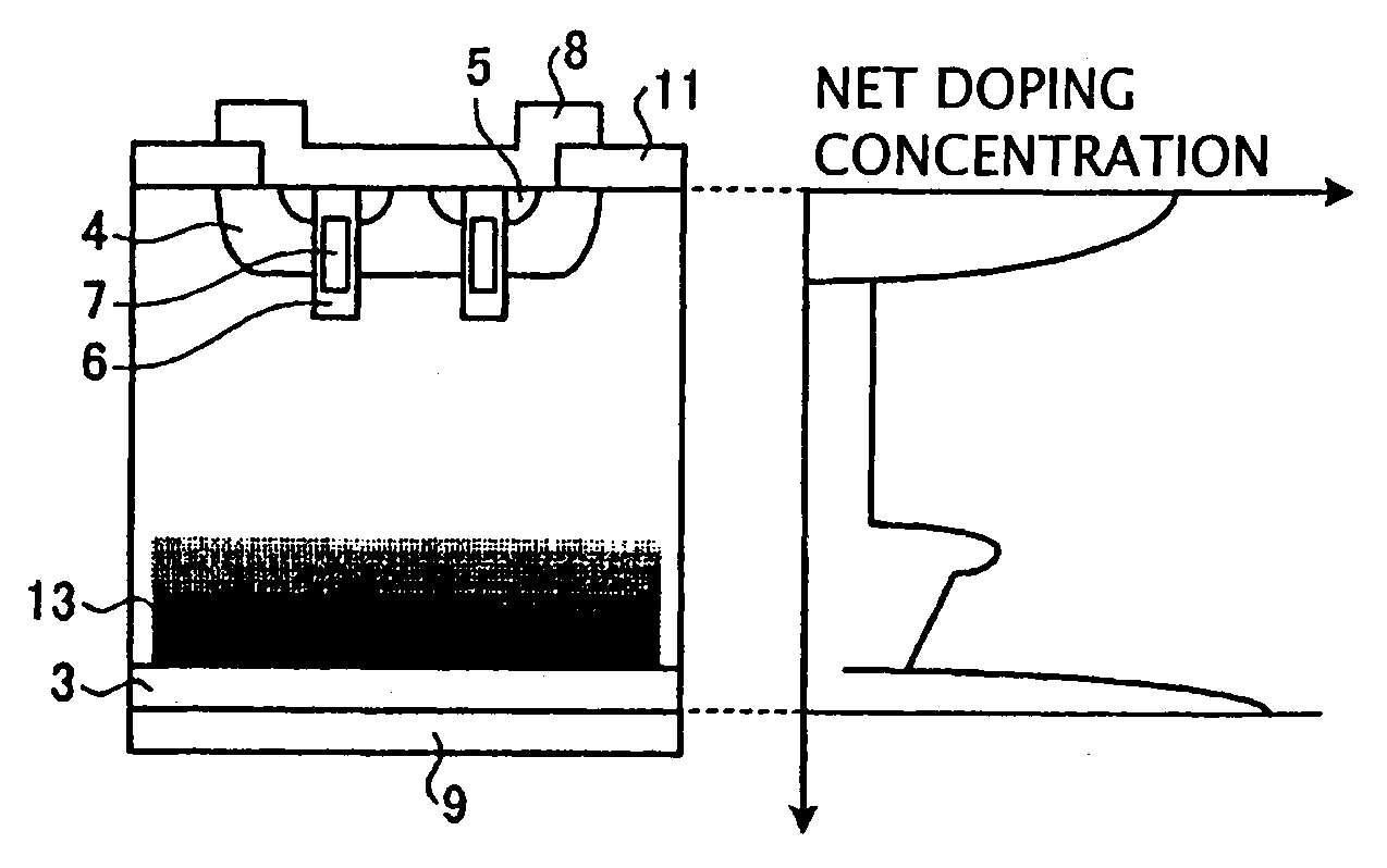
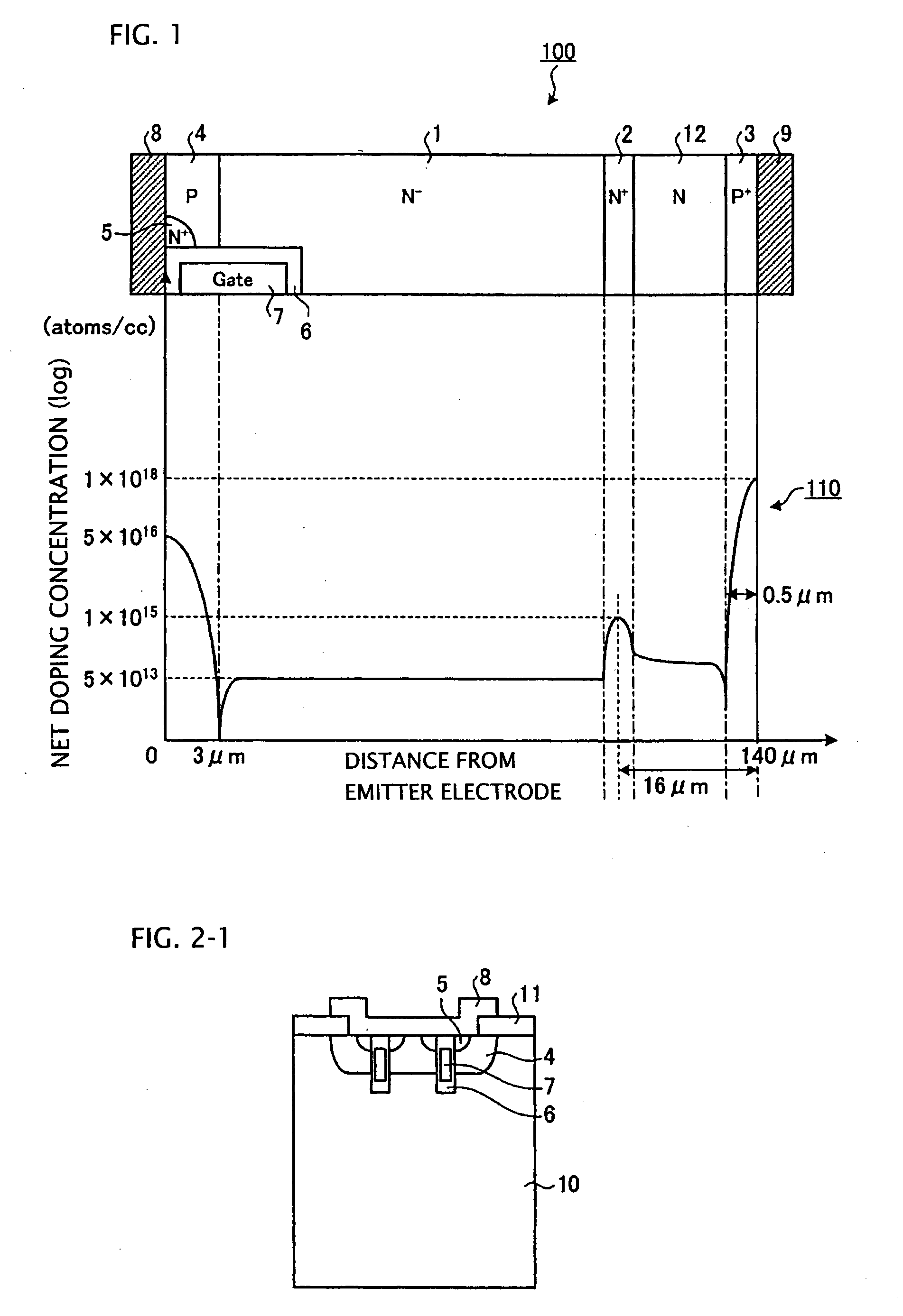
[0076]FIG. 1 is a view showing the configuration of a semiconductor device and the net doping concentration thereof. As shown in a section 100 of the semiconductor device in FIG. 1, for example, an N+ first buffer layer (N+ field stop layer) 2 as a second semiconductor layer, an N second buffer layer 12 as a third semiconductor layer and a P+ collector layer 3 as a fourth semiconductor layer are formed in this order on one principal surface (first principal surface) of an N− drift layer 1 as a first semiconductor layer. A P base layer 4 as a fifth semiconductor layer is formed on the other principal surface (second principal surface) of the N− drift layer 1. An N source layer 5 as a sixth semiconductor layer is formed in part of a surface layer of the P base layer 4 so as to be far from the N− drift layer 1. A gate electrode 7 is formed through a gate insulating film 6 in a trench which passes through the N source layer 5 and the P base layer 4 and reaches the N− drift layer 1. An ...

embodiment 2

[0138]It is hence to be understood that helium ions, lithium ions or oxygen ions are preferred as other elements to be injected than protons in accordance with As shown in FIG. 6 and FIGS. 11 to 13, it is found that the preferred acceleration voltage is 200 keV at minimum and 30 MeV at maximum and the preferred acceleration voltage for injection of protons is 2 MeV at maximum.

[0139]FIG. 14 is a view showing the configuration and net doping concentration of a semiconductor device according to Embodiment 3. As shown in a section 200 of the semiconductor device in FIG. 14, the semiconductor device according to Embodiment 3 includes, in addition to the semiconductor device of Embodiment 1 shown in FIG. 1, an N+ cathode buffer layer 22 (seventh semiconductor layer) provided between the N second buffer layer 12 and the P+ collector layer 3 and being higher in concentration than the N second buffer layer 12. The other configuration is the same as in Embodiment 1 and like numerals refer to...

embodiment 3

[0142], the depletion layer spread from the emitter side into the drift layer can be stopped more surely by the N+ cathode buffer layer 22 before the depletion layer reaches the P+ collector layer 3. Accordingly, the incomplete formation of the buffer layer can be prevented, so that the percentage of leakage current non-defective products can be improved more greatly.

[0143]FIG. 15 is a graph showing turn-off waveforms of the semiconductor device according to Embodiments 1 to 3 and the semiconductor device including the field stop layer according to the related art. In FIG. 15, the thick solid line expresses the collector current IC and collector-emitter voltage VC of the semiconductor device according to Embodiments 1 to 3. The thin broken line expresses the collector current IC and collector-emitter voltage VC of the semiconductor device including the field stop layer according to the related art (see FIG. 19).

[0144]All the turn-off waveforms shown in FIG. 15 are waveforms in a snu...


PUM


Abstract

A semiconductor device is provided in which a semiconductor substrate can be prevented from being broken while elements can be prevented from being destroyed by a snap-back phenomenon. After an MOS gate structure is formed in a front surface of an FZ wafer, a rear surface of the FZ wafer is ground. Then, the ground surface is irradiated with protons and irradiated with two kinds of laser beams different in wavelength simultaneously to thereby form an N+ first buffer layer and an N second buffer layer. Then, a P+ collector layer and a collector electrode are formed on the proton-irradiated surface. The distance from a position where the net doping concentration of the N+ first buffer layer is locally maximized to the interface between the P+ collector layer and the N second buffer layer is set to be in a range of 5 μm to 30 μm, both inclusively.

Description

BACKGROUND OF THE INVENTION[0001]The present invention relates to a semiconductor device such as a diode or an IGBT (Insulated Gate Bipolar Transistor) having soft recovery characteristics in addition to high-speed and low-loss characteristics, and a method for producing the semiconductor device.[0002]There are diodes or IGBTs of 600 V, 1200 V or 1700 V withstand voltage class as power semiconductor devices. Improvement of characteristics of these devices has advanced recently. The power semiconductor devices are used in power conversion systems such as a high-efficiency power-saving converter-inverter system and essential for controlling rotation motors and servomotors.[0003]Characteristics of low loss, power saving, high speed, high efficiency and environmental friendliness, that is, no bad influence on surroundings are required of such a power controller. For such requirements, there is commonly known a method of thinning a rear surface of a usual semiconductor substrate (e.g. si...

Claims


Application Information

Patent Timeline
Patent Type & Authority Applications(United States)
IPC IPC(8): H01L29/739H01L21/26
CPCH01L29/32H01L29/66348H01L21/263H01L29/36H01L29/7397H01L29/1095
Inventor NEMOTO, MICHIONAKAZAWA, HARUO
Owner FUJI ELECTRIC CO LTD
Why Eureka
Try Eureka