Mold for microlens and process for producing the same

a microlense and microlens technology, applied in the field of microlenses, can solve the problems of low efficiency of light convergence, low productivity, and low production methods of ordinary lenses, and achieve the effects of low cost, low material cost and low cos

Inactive Publication Date: 2009-08-06
TAKAMOTO KIICHI
View PDF4 Cites 20 Cited by
  • Summary
  • Abstract
  • Description
  • Claims
  • Application Information

AI Technical Summary

Benefits of technology

[0035](f) The material cost is low because a silicon substrate is used for the mold and microlenses and microlens arrays can be produced at a low cost although the lifetime may not be long.
[0036]A microlens according to the seventh aspect of the inven

Problems solved by technology

These production methods for ordinary lenses cannot be used for the production of microlenses with a small size.
In other words, technologies such as photolithography and electron beam lithography are used for the production, but the required accuracy in superposition is severe with photolithography, and electron beam lithography is disadvantageous in that patterning in a special shape such as a circle is required and that the productivity is low.
Microlenses of the diffraction type are also disadvantageous in that chromatic aberration is large and that the efficiency of light convergence is low.
Not only is this production method time-consuming, but it is also

Method used


Image

  • Mold for microlens and process for producing the same
  • Mold for microlens and process for producing the same
  • Mold for microlens and process for producing the same

Examples


Embodiment Construction

[0057]Embodiments of the invention are described next with reference to the drawings.

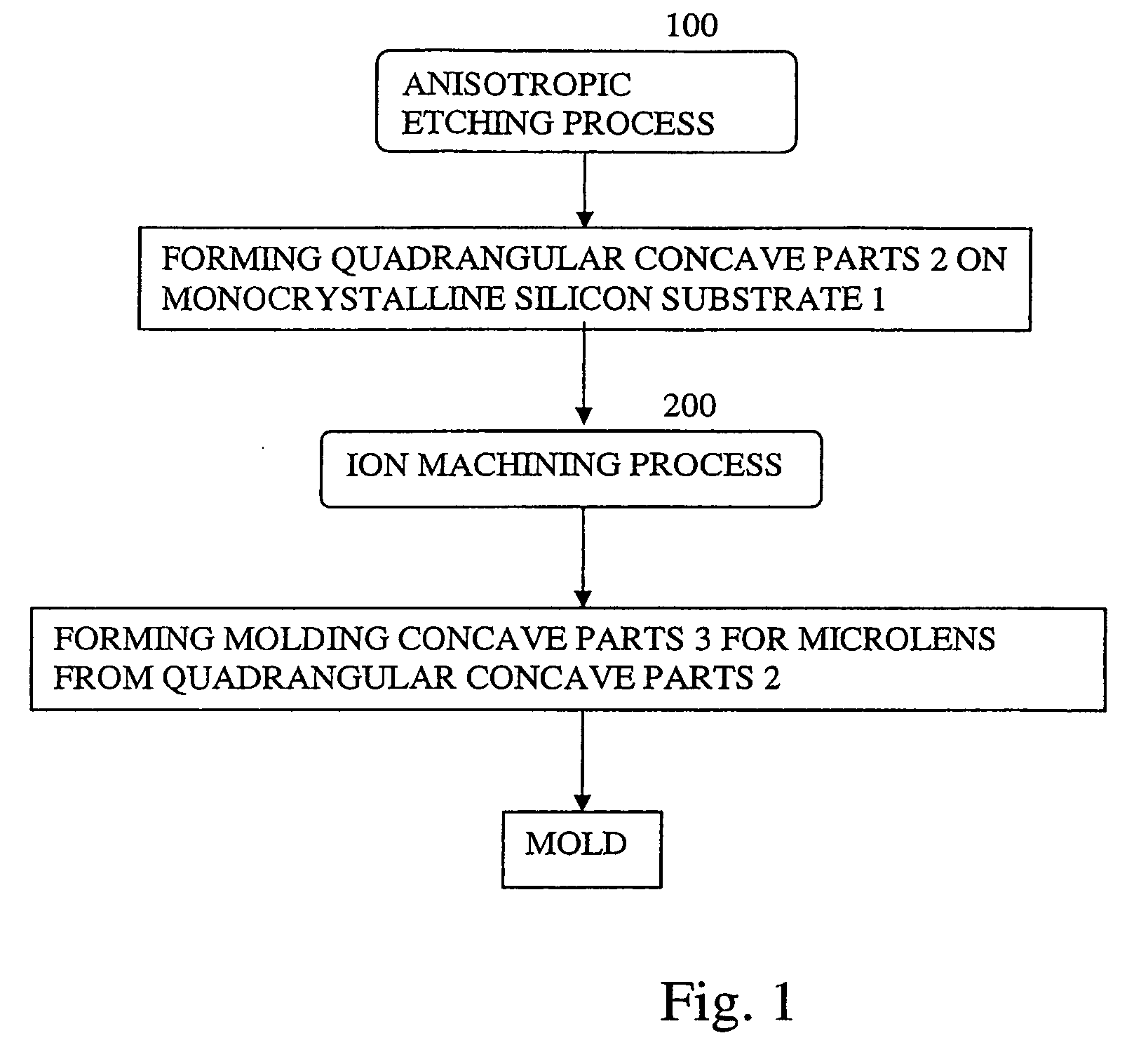
[0058]Basic principles of the production method of a mold for microlens according to this invention are explained first with reference to FIG. 1.

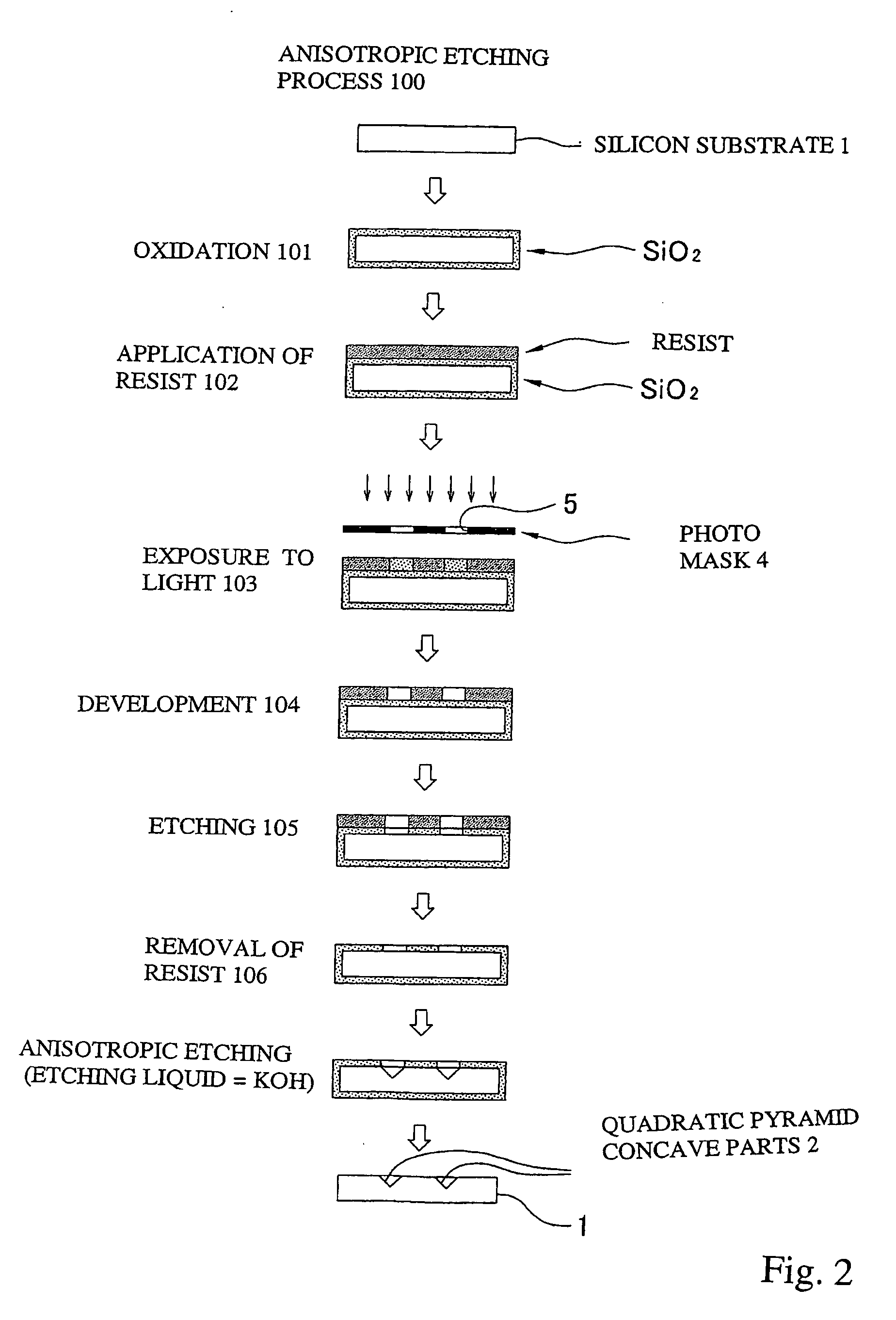
[0059]Firstly, a concave part hereinafter referred to as the quadrangular pyramid concave part 2 is formed on a single crystal silicon substrate 1 having a 100 crystal surface in an anisotropic etching process {100} using a chemical etching method. (See FIG. 2.) What is herein referred to as the quadrangular pyramid concave part 2, however, may be an indentation not only of a square shape but also of a rectangular shape in the plan view. In the case of an indentation with a square shape in the plan view, it is a normal pyramid shape with the top at one point. In the case of an indentation with a rectangular shape in the plan view, it is an indentation of a so-called wedge shape with the top having a finite length. The surfaces forming such indentations are ...


PUM

PropertyMeasurementUnit
Linear densityaaaaaaaaaa

Abstract

A mold for producing microlenses or a microlens array is produced by sequentially carrying out an etching step of forming quadrangular pyramid concave parts on a single crystal silicon substrate by anisotropic etching and an ion etching step of forming molding concave parts with spherical or cylindrical surface parts from the quadrangular pyramid concave parts.

Description

[0001]This application is a continuation of International Application No. PCT / JP2006 / 316152, filed Aug. 17, 2006 which claims priority on Japanese Patent Application 2005-238596 filed Aug. 19, 2005.BACKGROUND OF THE INVENTION[0002]This invention relates to a mold for microlens, a process for its production and microlens. Small lenses with diameters less than a few millimeters are referred to as microlenses. Several of them may be formed in a neatly arranged array or they may be used singly, as disclosed in Optoelectronics Technical Dictionary (edited by Shunichi Tanaka, et al. and published by Ohm Publishing Co. (1996)). This invention relates to a mold that may be used for the production of such a microlens, a process for its production and microlens.[0003]Throughout herein, the term “microlens” may be used to indicate both a single microlens and a microlens array, especially they are not particularly distinguished.[0004]Lenses for cameras and optical microscopes are produced by po...

Claims


Application Information

Patent Timeline
IPC IPC(8): B28B7/34B44C1/22G02B3/00
CPCB29C33/3842B29C33/424G02B3/0018B29L2011/0016B29D11/00365
Inventor TAKAMOTO, KIICHI
Owner TAKAMOTO KIICHI
Why Eureka
Try Eureka