Method for Manufacturing Bonded Substrate

a technology of bonded substrate and manufacturing method, which is applied in the direction of basic electric elements, electrical apparatus, semiconductor devices, etc., can solve the problems of reducing the yield of devices, the diameter of the entire bonded substrate becomes small, and the inability to use existing facilities and jigs, etc., to achieve excellent edge portion shape and reduce the film thickness of the bonded substrate

Inactive Publication Date: 2009-08-13
SHIN-ETSU HANDOTAI CO LTD
View PDF5 Cites 29 Cited by
  • Summary
  • Abstract
  • Description
  • Claims
  • Application Information

AI Technical Summary

Benefits of technology

[0031]As explained above, in the method for manufacturing a bonded substrate according to the present invention, even if the groove is provided after mirror polishing, the unbonded portion in the active layer wafer outer peripheral portion can be removed. In particular, when forming the oxide film on the surface of the active layer wafer, forming the groove after formation of the oxide film following mirror polishing is preferable.
[0032]As explained above, according to the present invention, the operat

Problems solved by technology

Furthermore, when such a bonded substrate is subjected to a device process, the remaining unbonded portion is delaminated in the device process, and particles are generated, thereby reducing a device yield.
However, the above-explained methods have the following inconveniences.
That is, in the method disclosed in Japanese Patent Application Laid-open No. 1986-256621, there occurs a problem that a diameter of the entire bonded substrate becomes small and existing facilities and jigs cannot be used as they are.
Furthermore, Japanese Patent Application Laid-open No. 1989-227441 has a problem that etching must be carried out and the number of processes is increased since a damaged layer is produced due to grinding and that a wafer shape varies since grinding is carried out until reaching a portion near a periph

Method used


Image

  • Method for Manufacturing Bonded Substrate
  • Method for Manufacturing Bonded Substrate
  • Method for Manufacturing Bonded Substrate

Examples


example 1

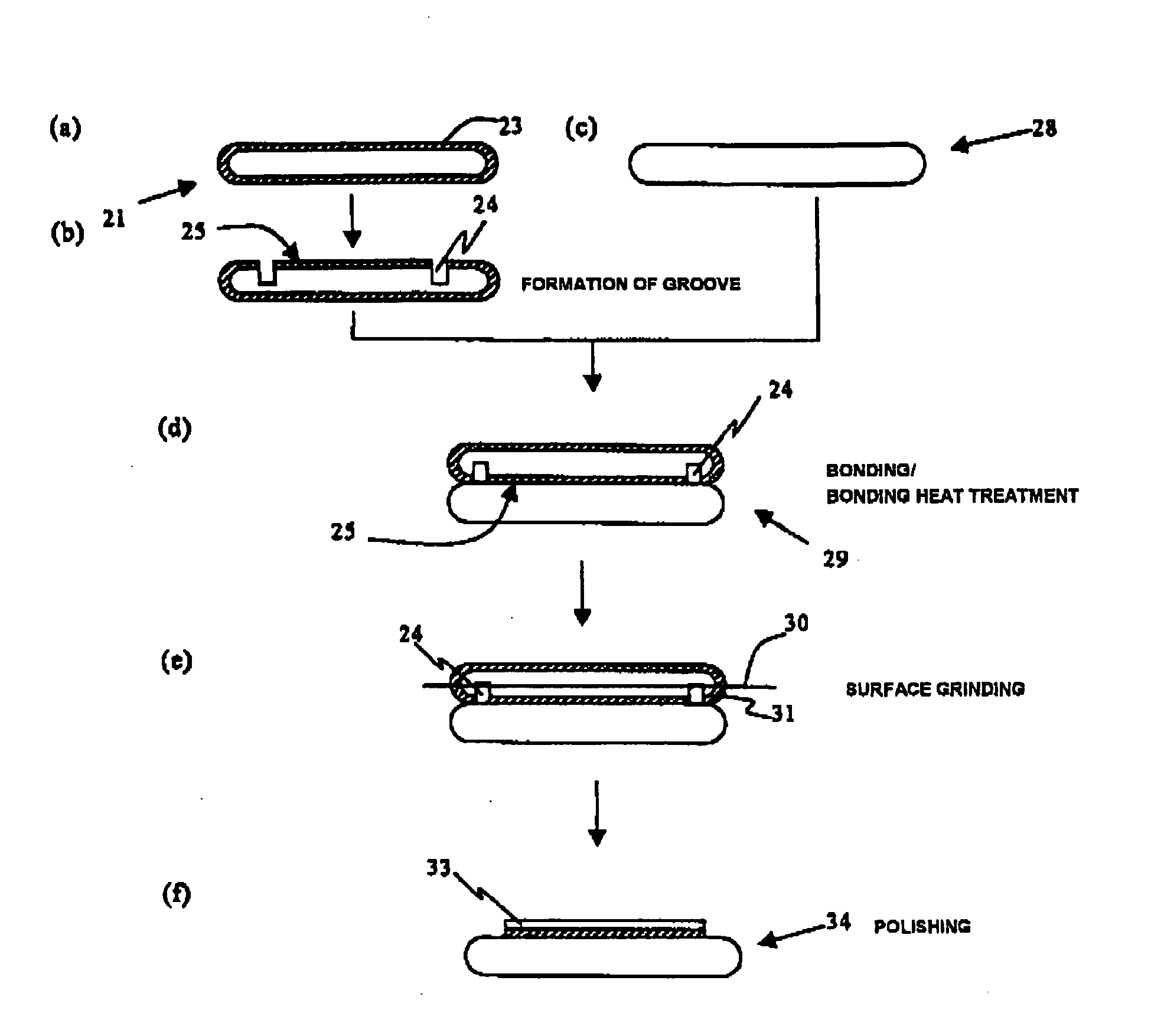
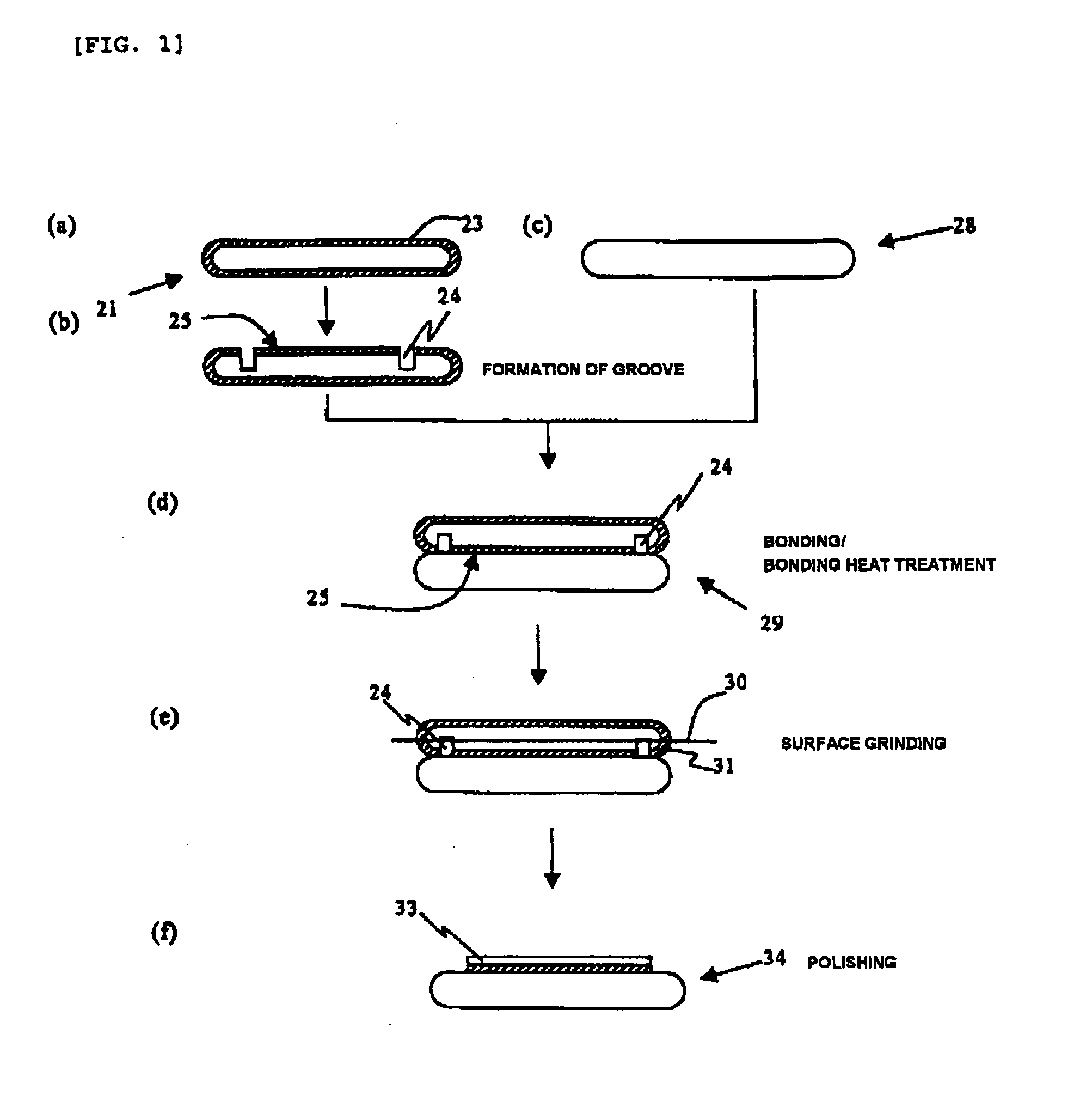
[0084]A description will be first given on a method for reducing a film thickness of an active layer wafer based on surface grinding after the active layer wafer is bonded to a support substrate wafer.

[0085]A p-type single crystal silicon ingot having a resistance of 8 to 12 Ωcm pulled up by a Czochralski method was sliced to obtain a thin discoid wafer having a diameter of 150 mm (6 inches) and a thickness of 625 μm. An outer edge portion was chamfered to avoid breakage, cracks, and particle generation in the wafer, and then lapping was carried out to flatten the wafer. Subsequently etching was performed to remove a mechanical damage remaining on a surface of the lapped wafer. Further, primary mirror polishing was performed with respect to both front and back surfaces of the wafer, and a chamfer portion was also polished.

[0086]As explained above, the silicon wafer was subjected to primary mirror polishing, thereby providing an active layer wafer. A water jet guided laser was used ...

example 2

[0091]A description will now be given as to a method for reducing a film thickness of an active layer wafer after bonding the active layer wafer to a support substrate wafer based on an ion implantation and delamination method.

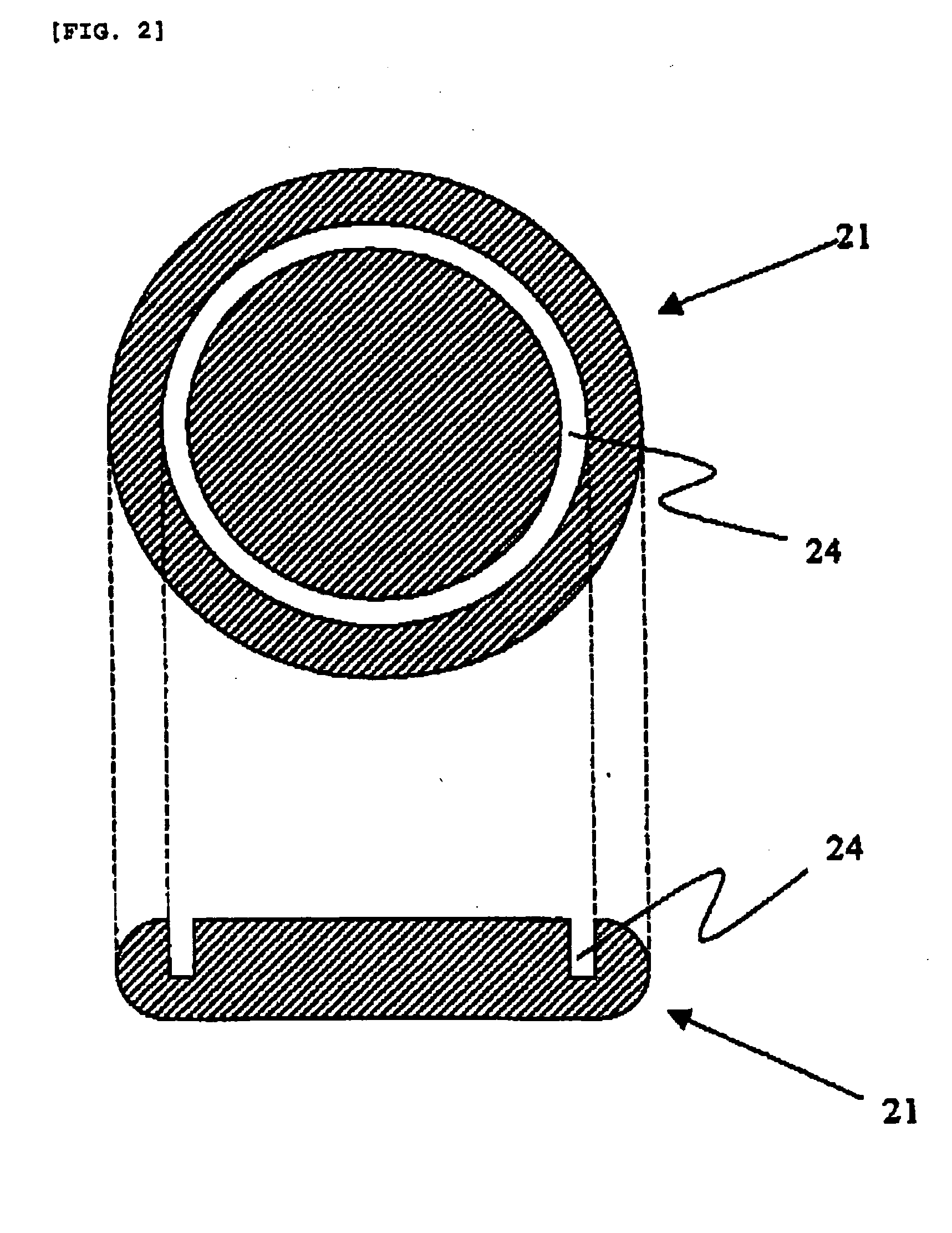
[0092]First, like Example 1, the silicon wafer was subjected to primary mirror polishing to provide an active layer wafer. A water jet guided laser was used with respect to this wafer to form a groove having a groove width of 100 μm and a groove depth of 10 μm in a region of a wafer periphery that is 1 mm apart from an outer periphery long the outer periphery as shown in FIG. 2. As a condition of the water jet guided laser at this step, a long-cycle pulse having a wavelength of 1064 nm was used. After forming the groove, mirror finishing was effected.

[0093]Subsequently, this active layer wafer was subjected to a heat treatment in an oxidizing atmosphere to form an oxide film on an entire surface of the wafer. This active layer wafer was subjected to hydrogen i...


PUM


Abstract

The present invention provides a method for manufacturing a bonded substrate that is a method for manufacturing a bonded substrate where an active layer wafer is bonded to a support substrate wafer, comprising: a first step of providing a groove on an inner side on a surface of the active layer wafer along an outer peripheral portion over an entire circumference; a second step of determining a surface where the groove is formed as a bonding surface and bonding the active layer wafer to the support substrate wafer; and a third step of reducing a film thickness of the active layer wafer and removing an unbonded portion on an outer side of the groove of the active layer wafer. As a result, there is provided the method for manufacturing a bonded substrate that can simplify processes, avoid breakage, cracks, or particle generation, and manage a shape of an edge portion of an active layer wafer when reducing a film thickness of the active layer wafer.

Description

TECHNICAL FIELD[0001]The present invention relates to a method for manufacturing a bonded substrate by bonding an active layer wafer to a support substrate wafer and then reducing a film thickness of the active layer wafer, e.g., a method for manufacturing a bonded substrate such as a directly bonded substrate or an SOI substrate.BACKGROUND ART[0002]As a semiconductor substrate for a high-performance device, a bonded substrate obtained by bonding an active layer wafer to a support substrate wafer and then reducing a film thickness of the active layer wafer is used. As one of such bonded substrates, an SOI substrate is known.[0003]As a method for manufacturing the SOI substrate, the following method is known, for example. That is, two mirror-polished silicon wafers (an active layer wafer and a support substrate wafer) are prepared, and an oxide film is formed on at least one of the wafers. These wafers are bonded to each other through the oxide film and then subjected to a heat treat...

Claims


Application Information

Patent Timeline
IPC IPC(8): H01L21/50
CPCH01L21/76256H01L21/76254H01L21/20H01L27/12H01L21/304H01L21/02
Inventor MITANI, KIYOSHI
Owner SHIN-ETSU HANDOTAI CO LTD
Why Eureka
Try Eureka