
Electrically-Pumped Semiconductor Zigzag Extended Cavity Surface Emitting Lasers and Superluminescent Leds

a laser and superluminescent technology, applied in semiconductor lasers, laser optical resonator construction, laser details, etc., can solve the problems of difficult to achieve high power output from large area and volume of gain material, design to suppress parasitic lasing is common, and the geometry of zigzag lasers has previously proved impractical for implementing efficient, etc., to achieve the effect of amplifying power

Active Publication Date: 2009-08-20
PHILIPS LUMILEDS LIGHTING CO LLC +1
View PDF10 Cites 31 Cited by
  • Summary
  • Abstract
  • Description
  • Claims
  • Application Information

AI Technical Summary

Benefits of technology

[0070]One advantage of the present invention is that it can be used to achieve surface emitting lasers in the GaN materials system. The GaN materials system is of interest to achieve visible and UV wavelength lasers. Conventionally these materials provide insufficient optical gain to achieve a high power surface emitting laser. However, in the present invention, the number of individual regenerative gain elements can be increased until the ZECSEL supports lasing at a desired wavelength in the GaN materials system.

Problems solved by technology

In contrast, a zigzag laser geometry has previously proven impractical for implementing an efficient, high power semiconductor laser with desirable optical mode characteristics.
It is difficult to achieve high power output from large area and volumes of gain material without creating various optical instabilities in the spatial and longitudinal modes.
As a result, because of the large gain in typical semiconductor materials, the design to suppress parasitic lasing is a common issue.
There are also practical difficulties in modulating a large area semiconductor laser due to their large capacitance (large RC time constant), the requirement for high modulation currents and the generation of various modal instabilities.
However, each of them has significant shortcomings that make them unusable as a practical alternative to other types of semiconductor lasers.
One approach to implementing a zigzag semiconductor laser is disclosed in U.S. Pat. Pub. 2003 / 0012246 by Klimek, “Semiconductor ZigZag Laser and Optical Amplifier.” However, the numerous deficiencies in Klimek make the design unusable for achieving an efficient, electrically pumped laser with a stable large-area optical mode.
Klimek describes both optical pumping and electrical pumping but does not disclose a practical means to provide efficient electrical pumping.
Thus, in electrically pumped embodiments of Klimek the optical mode traverses a zigzag path through both n and p doped active regions and n and p doped cladding regions, resulting in significant optical loss.
As a result gain is not utilized effectively.
Additionally, there are also several other practical problems with the electrically pumped embodiments disclosed in Klimek.
However, there are practical limits to the thickness with which doped cladding layers can be grown with a high optical and material quality and with a reasonably low electrical resistance consistent with an efficient design.
However, if such an efficient laser structure was used in Klimek it would limit the vertical mode to a few microns in dimension, i.e., to a dimension consistent with bouncing the mode within a laser structure having cladding layers of only a few microns in thickness.
Klimek also does not disclose a practical means to couple light into and out of the semiconductor chip.
While Klimek discloses one embodiment with angled facets, such angled facets are difficult to fabricate with controlled angles in most semiconductors.
However, such micro-prisms would be difficult to implement on such a small physical scale and would require additional alignment and packaging steps that are undesirable.
However, this will tend to result in the generation of multiple lateral modes in the laser, similar to that observed in large area edge-emitting lasers, or as one extreme would result in parasitic lateral lasing.
Klimek also does not provide guidelines for practical dimensions of its proposed structures and offers no solutions for dissipating and removing heat from the laser and for addressing stresses in the epitaxial structure.
Klimek also has other deficiencies, including non-operative examples in which the stated materials would not have the correct indices of refraction to provide total internal reflection.
The Mooradian patent does not, however, utilize total internal reflection.
First, the use of optical gain is potentially inefficient, as the entire amplifier is pumped whereas the zigzag path will result in a sequence of nodes and antinodes along the gain region due to the zigzag path.
Second, the spot size will be limited to a comparatively small spot size.
In light of these various considerations, the amplifier cannot be used as the basis of an efficient, high-power laser with a large spot size.
Thus, while the prior art suggests a long-felt need for a zigzag-type semiconductor laser with desirable beam characteristics this objective has not been met.
The solutions proposed in the prior art are not consistent with achieving an electrically pumped semiconductor laser that is efficient, capable of high power output, which has a large spot size and which can be effectively used in a gain-switched or mode-locked configuration.

Method used


Image

  • Electrically-Pumped Semiconductor Zigzag Extended Cavity Surface Emitting Lasers and Superluminescent Leds
  • Electrically-Pumped Semiconductor Zigzag Extended Cavity Surface Emitting Lasers and Superluminescent Leds
  • Electrically-Pumped Semiconductor Zigzag Extended Cavity Surface Emitting Lasers and Superluminescent Leds

Examples


Embodiment Construction

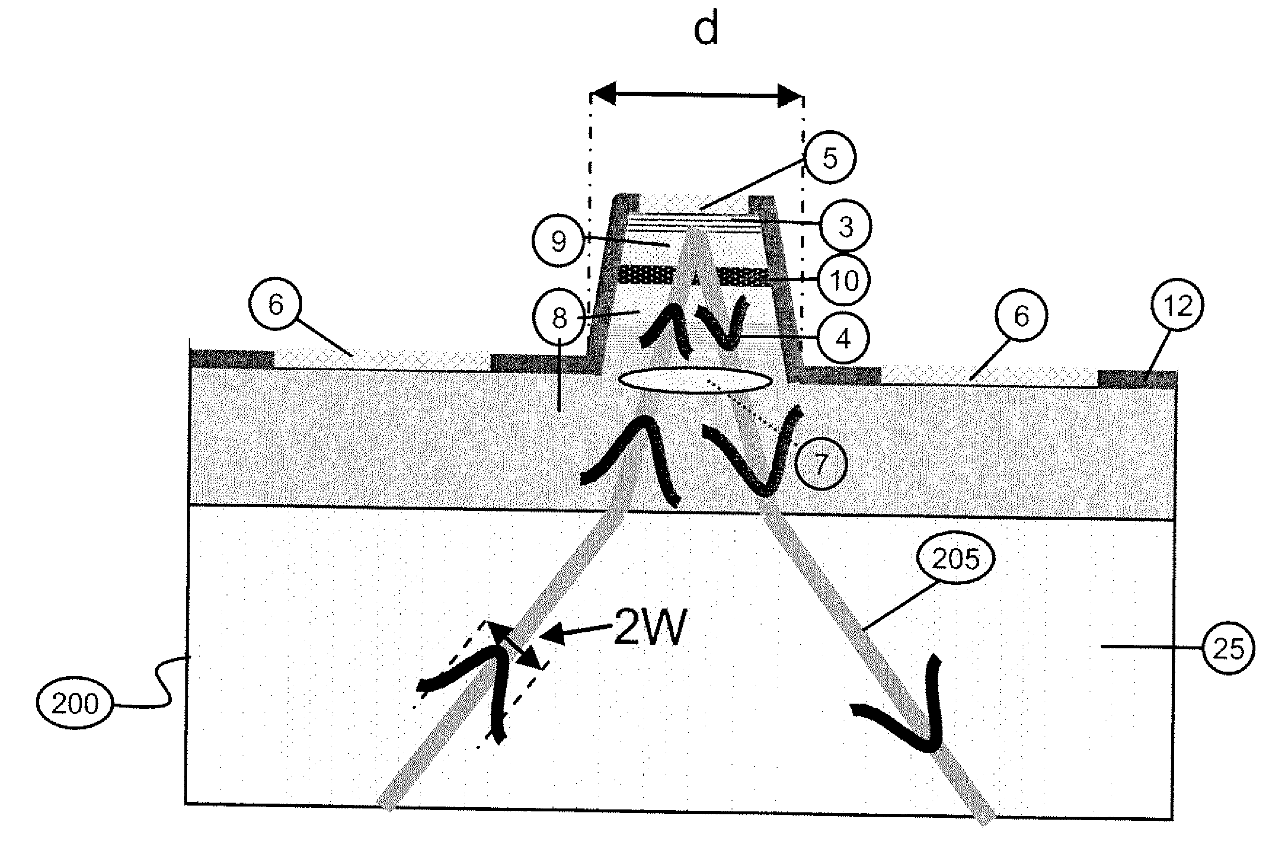
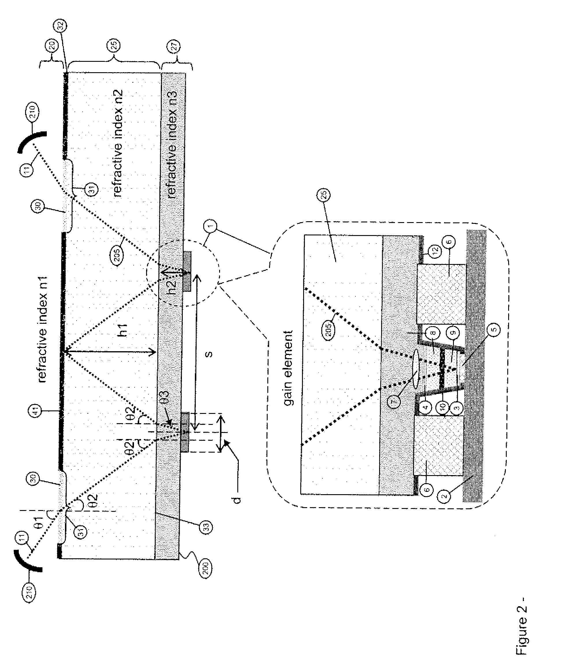
[0028]Embodiments of the present invention are directed to new types of high brightness surface emitting semiconductor lasers and superluminescent LEDs using a single chip optical amplifier having a plurality of electrically pumped semiconductor gain elements optically coupled to each other by a zigzag optical path within a low optical loss substrate. The optical amplifier chip permits a higher cumulative optical gain than is possible with an individual gain element, which supports high power amplifier or laser operation and the use of a wide variety of different semiconductor materials at different wavelengths, including the blue and ultraviolet. Additionally, individual gain elements may be separately modulated as reverse-biased p-n junction modulators to adjust the optical loss for gain-switching or mode-locking. The optical amplifier chip has applications that include its use as a surface emitting laser, a superluminescent LED (SLED), intra-cavity frequency doubled laser, or ext...


PUM


Abstract

A semiconductor surface emitting optical amplifier chip utilizes a zigzag optical path within an optical amplifier chip. The zigzag optical path couples two or more gain elements. Each individual gain element has a circular aperture and includes a gain region and at least one distributed Bragg reflector. In one implementation the optical amplifier chip includes at least two gain elements that are spaced apart and have a fill factor no greater than 0.5. As a result the total optical gain may be increased. The optical amplifier chip may be operated as a superluminescent LED. Alternately, the optical amplifier chip may be used with external optical elements to form an extended cavity laser. Individual gain elements may be operated in a reverse biased mode to support gain-switching or mode-locking.

Description

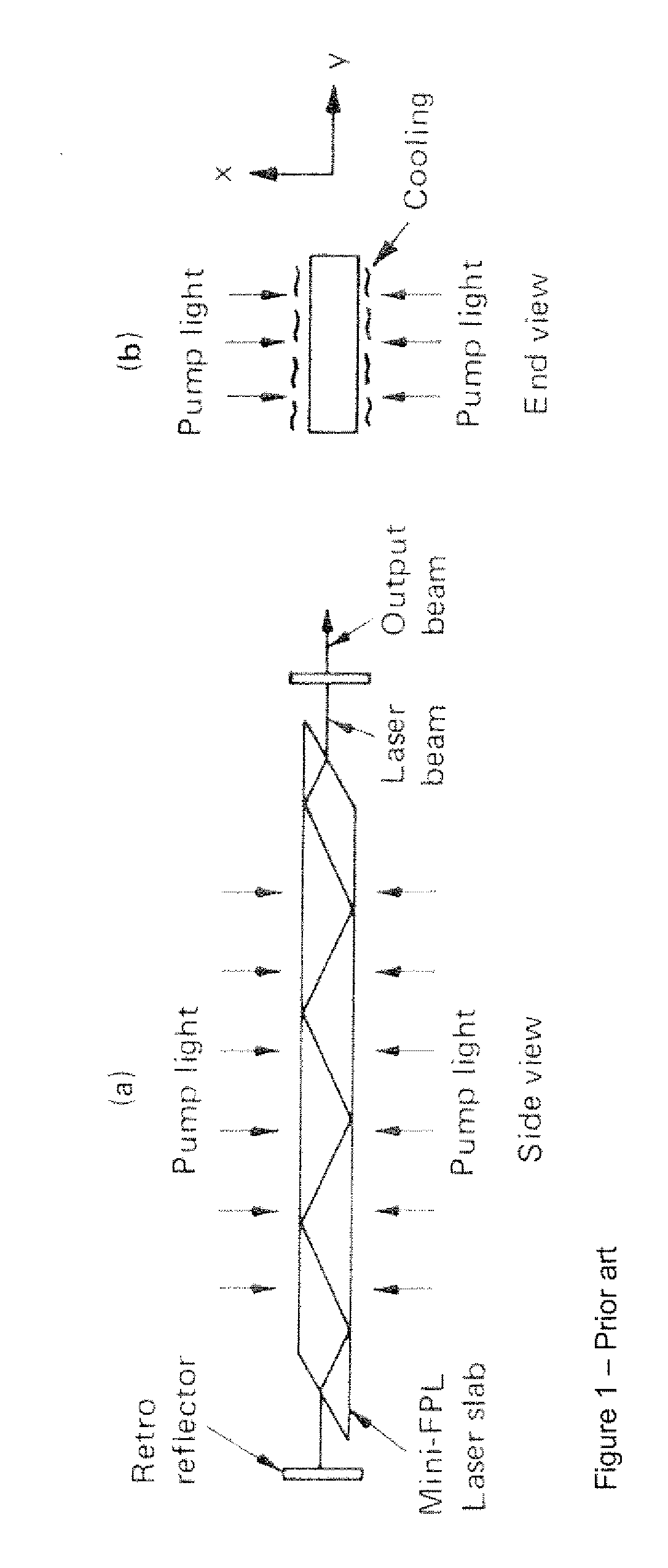
CROSS-REFERENCE TO RELATED APPLICATIONS[0001]This application claims the benefit of U.S. provisional patent application No. 61 / 065,817 filed on Feb. 14, 2008 which application is hereby incorporated by reference in its entirety.FIELD OF THE INVENTION[0002]The present invention is generally related to semiconductor surface emitting lasers. More particularly the present invention is directed towards improving the performance of extended cavity surface emitting semiconductor laser structures by using a zigzag configuration.BACKGROUND OF THE INVENTION[0003]Optically pumped solid state Nd:YAG slab lasers arc an important class of solid state lasers. One type of Nd:YAG slab laser is a zigzag slab geometry, illustrated in FIG. 1. In the zigzag slab geometry the Nd:YAG slab has a rectangular cross-section. The slab includes tilted facets to permit a laser beam to enter and exit the slab. The slab has two large opposing faces. As illustrated in prior art FIG. 1, the slab is optically pumped ...

Claims


Application Information

Patent Timeline
Patent Type & Authority Applications(United States)
IPC IPC(8): H01S5/323H01S5/02315
CPCH01S3/109H01S5/005H01S5/0092H01S5/02236H01S5/02296H01S5/026H01S5/5081H01S5/14H01S5/183H01S5/423H01S5/5018H01S5/5036H01S5/0286H01S5/0233H01S5/0235H01S5/02257H01S5/18305H01S5/02315
Inventor JANSEN, MICHAEL
Owner PHILIPS LUMILEDS LIGHTING CO LLC
Learn More