Scanning Electron Microscope system and Method for Measuring Dimensions of Patterns Formed on Semiconductor Device By Using the System

a scanning electron microscope and pattern technology, applied in the field of pattern image measurement system, can solve the problems of low accuracy of opc verification, mislead adjustment amount of correction pattern size, and all consider capturing the pattern edge end correctly, and achieve the effect of high reliability of dimension measuremen

Active Publication Date: 2009-08-27
HITACHI HIGH-TECH CORP
View PDF3 Cites 20 Cited by
  • Summary
  • Abstract
  • Description
  • Claims
  • Application Information

AI Technical Summary

Benefits of technology

[0015]The present invention is for providing a scanning electron microscope system capable of extracting contour information fitting in with the real pattern edge end of the sample, thereby performing highly reliable dimension measurement.

Problems solved by technology

However, JP-A-2007-121147 and JP-A-2001-338304 do not at all consider capturing the pattern edge end correctly.
What is further problematical is the fact that the distance between the edge position detected in FIGS. 5C and 5D and the bottom end varies depending on the cross-sectional shape of the pattern (between the region A and region B in the drawing).
In the situation in which the pattern edge end is not detected correctly as described above, the adjustment amount of the correction pattern size might be misled, and it is obvious that the highly accurate OPC verification is not achieved.

Method used


Image

  • Scanning Electron Microscope system and Method for Measuring Dimensions of Patterns Formed on Semiconductor Device By Using the System
  • Scanning Electron Microscope system and Method for Measuring Dimensions of Patterns Formed on Semiconductor Device By Using the System
  • Scanning Electron Microscope system and Method for Measuring Dimensions of Patterns Formed on Semiconductor Device By Using the System

Examples


first embodiment

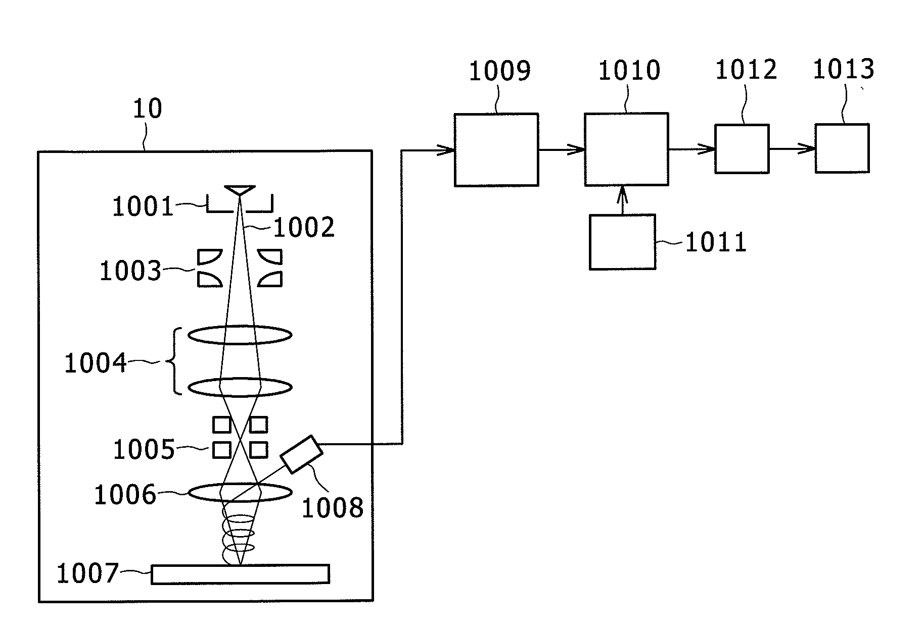
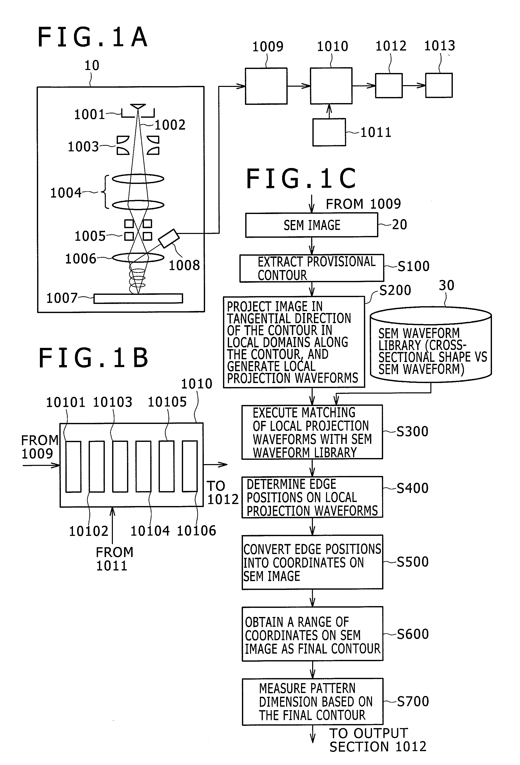
[0042]A flow of shape measurement in a semiconductor wafer shape measurement device according to the present invention is shown in FIGS. 1A through 1C.

[0043]Firstly, an acquisition method of an SEM image using an SEM device 10 will be explained with reference to FIG. 1A. An electron beam 1002 emitted from an electron gun 1001 of the SEM 10 is accelerated by an acceleration electrode 1003, then converged by a convergent lens 1004, scanned by a deflector 1005 in X and Y directions (in a plane perpendicular to the sheet of the drawing in FIG. 1A), focused by an objective lens 1006 on a surface of a sample 1007 provided with a measurement object patterns, so as to illuminate the surface of the sample 1007 in a scanning manner. Although omitted from illustration in FIG. 1A, the sample 1007 is mounted on a table so as to be movable in a plane, and is controlled so that a desired area of the surface of the sample 1007 is positioned in the irradiation range of the electron beam 1002.

[0044]A...

second embodiment

[0060]FIG. 10B is a flowchart of the shape measurement according to a second embodiment of the present invention. Although the configuration of the SEM system in the present embodiment is basically the same as the configuration shown in FIG. 1A explained in the first embodiment, the configuration of the operation section 1010 is slightly different.

[0061]FIG. 10A shows the configuration of the operation section 1020 in the present embodiment. The operation section 1020 is provided with a provisional contour extraction section 10201, a local projection waveform forming section 10202, a characteristic value calculation section 10203, a representative point extraction section 10204, a library matching section 10205, an edge determination section 10206, a coordinate conversion / contour extraction section 10207, and a dimension measurement section 10208.

[0062]Hereinafter, each of the steps will be explained along the flowchart shown in FIG. 10B.

[0063](S110): Similarly to the step S100 in t...

third embodiment

[0078]FIG. 14 is a flowchart of the shape measurement according to a third embodiment of the present invention. Although the flow of the shape measurement according to the present embodiment is basically the same as the case with the first embodiment explained using FIG. 1C, the present embodiment is different from the first and second embodiments in that an SEM waveform characteristic value library 31, which includes the cross-sectional shapes 701′ of the pattern and characteristic values obtained from the SEM waveforms 702′ correlated with each other, is stored in the storage section 1011, and is used for estimating the cross-sectional shape from the local projection waveform, in contrast that in the first and second embodiments, the library 30 including the cross-sectional shapes 701 of the pattern and the SEM waveforms 702 correlated with each other, and stored in the storage section 1011 is used for estimating the cross-sectional shape from the local projection waveform. In oth...


PUM

PropertyMeasurementUnit
heightaaaaaaaaaa
scanning electron microscopeaaaaaaaaaa
areaaaaaaaaaaa

Abstract

The present invention is for providing a scanning electron microscope system adapted to output contour information fitting in with the real pattern edge end of a sample, and is arranged to generate a local projection waveform by projecting the scanning electron microscope image in the tangential direction with respect to the pattern edge at each point of the pattern edge of the scanning electron microscope image, estimate the cross-sectional shape of the pattern transferred on the sample by applying the local projection waveform generated at each point to a library, which has previously been created, correlating the cross-sectional shape with the electron beam signal waveform, obtain position coordinate of the edge end fitting in with the cross-sectional shape, and output the contour of the pattern as a range of position coordinates.

Description

CLAIM OF PRIORITY[0001]The present application claims priority from Japanese application serial no. JP2008-040816, filed on Feb. 22, 2008, the content of which is hereby incorporated by reference into this application.1. BACKGROUND OF THE INVENTION[0002]The present invention relates to a pattern image measurement system adapted to measure a pattern image obtained by imaging a photo mask used in a lithography process of semiconductor manufacturing or a wafer having been processed by the lithography process with a scanning electron microscope.2. RELATED ART[0003]Due to the miniaturization of semiconductor circuit patterns, the resolution of exposure devices reaches a limit, and in order for forming the circuit patterns on a silicon wafer as designed, an Optical Proximity Correction (OPC) process for previously putting correction patterns into the design data of the photo mask thereby controlling the finished shapes thereof is becoming in heavy use.[0004]The OPC patterns are designed b...

Claims


Application Information

Patent Timeline
Patent Type & Authority Applications(United States)
IPC IPC(8): G01N23/00G01B15/00G03F1/84H01L21/027
CPCG03F1/0092G03F7/70625G03F1/86G03F1/84
Inventor SHISHIDO, CHIETANAKA, MAKIMIYAMOTO, ATSUSHI
Owner HITACHI HIGH-TECH CORP
Why Eureka
Try Eureka