
Projection electron beam apparatus and defect inspection system using the apparatus

a technology of electron beam and projection electron beam, which is applied in the direction of magnetic discharge control, instruments, therapy, etc., can solve the problems of axial chromatic aberration, axial chromatic aberration increase, and discharge between a sample and the lens

Inactive Publication Date: 2009-08-27
KK TOSHIBA
View PDF18 Cites 72 Cited by
  • Summary
  • Abstract
  • Description
  • Claims
  • Application Information

AI Technical Summary

Benefits of technology

The present invention relates to an electron beam apparatus and a defect inspection system using the apparatus. The invention aims to provide an electron beam apparatus that can evaluate a sample with a pattern width of 0.25 μm or less with high accuracy and high throughput. The invention also aims to reduce the occurrence of discharges between the sample and the objective lens, and to improve the transmittance of secondary electrons. The invention addresses the limitations of conventional electron beam apparatuses and proposes an electron beam apparatus that can overcome these limitations and provide a higher resolution and higher throughput defect inspection system.

Problems solved by technology

For this reason, the electric field strength must be set to be relatively small, resulting in a problem of relatively large axial chromatic aberration.
Accordingly, when a low voltage is employed, axial chromatic aberration increases.
When the electric field strength is increased in order to reduce the axial chromatic aberration, a problem arises in that a discharge occurs between a sample and the lens.
Anyway, the transmittance of secondary electrons is difficult to be increased, as a consequence.
In this event, problems lie in that an axial magnetic field is not zero on the surface of a sample, and secondary electron beams emitted from the sample in the normal direction do not intersect with the optical axis or pass through an NA aperture.
Also, a MOL scheme has problems that a beam must be scanned, and it is hardly compatible with an inspecting device.
Further, in a rectangular visual field, problems are a long distance from the optical axis for the area, and large astigmatism.
Another problem lies in that a second electron beam is blurred by space charges of a primary electron beam.
Conventionally, when an LaB6 cathode is operated in a space charge limiting region, there is an advantage of small shot noise, but on the contrary, there is a problem of large chromatic aberration due to a large energy width.
However, the electron beam based defect inspection apparatus is disadvantageously inferior to the optical one in regard to the throughput.
In addition, the electron beam scheme is largely characterized by its abilities to inspect for electric defects (disconnected wires, defective conduction, defectively connected vias, and the like), but merely provides a very low inspecting speed.
However, in scanning a plurality of beams, no clear solution has been provided in regard to how a plurality of beams should be arranged in order to most effectively perform evaluations.
Moreover, the electron beam apparatus has a problem in that if a magnetic lens is employed for an objective lens, secondary electrons emitted from a sample in the normal direction to the surface of the sample do not intersect with the optical axis.

Method used


Image

  • Projection electron beam apparatus and defect inspection system using the apparatus
  • Projection electron beam apparatus and defect inspection system using the apparatus
  • Projection electron beam apparatus and defect inspection system using the apparatus

Examples


example

[0289]Indicated Direction: Right . . . Stage Moving Direction: Left (an image moves to the left=the field of view moves to the right)

[0290]Indicated Direction: Upward . . . Stage Moving Direction: Downward (an image moves downward=the field of view moves upward)

(2) Direct Entry of Coordinates on GUI:

[0291]Coordinates directly entered on the GUI are regarded as a location at which the operator wishes to view on the wafer coordinate system, so that the stage is moved such that the coordinate on a wafer are displayed at the center of a captured image.

[0292]In the apparatus described in connection with FIG. 14, a procedure is taken to mount a correction ring on the electrostatic chuck, and position a wafer such that the wafer fits in the inner diameter of the correction ring. Therefore, in the inspection apparatus illustrated in FIG. 15, a procedure is taken to mount a correction ring on a wafer in the load lock chamber 22•1, integrally transfer the wafer mounted with the correction rin...


PUM

PropertyMeasurementUnit
widthaaaaaaaaaa
widthaaaaaaaaaa
widthaaaaaaaaaa

Abstract

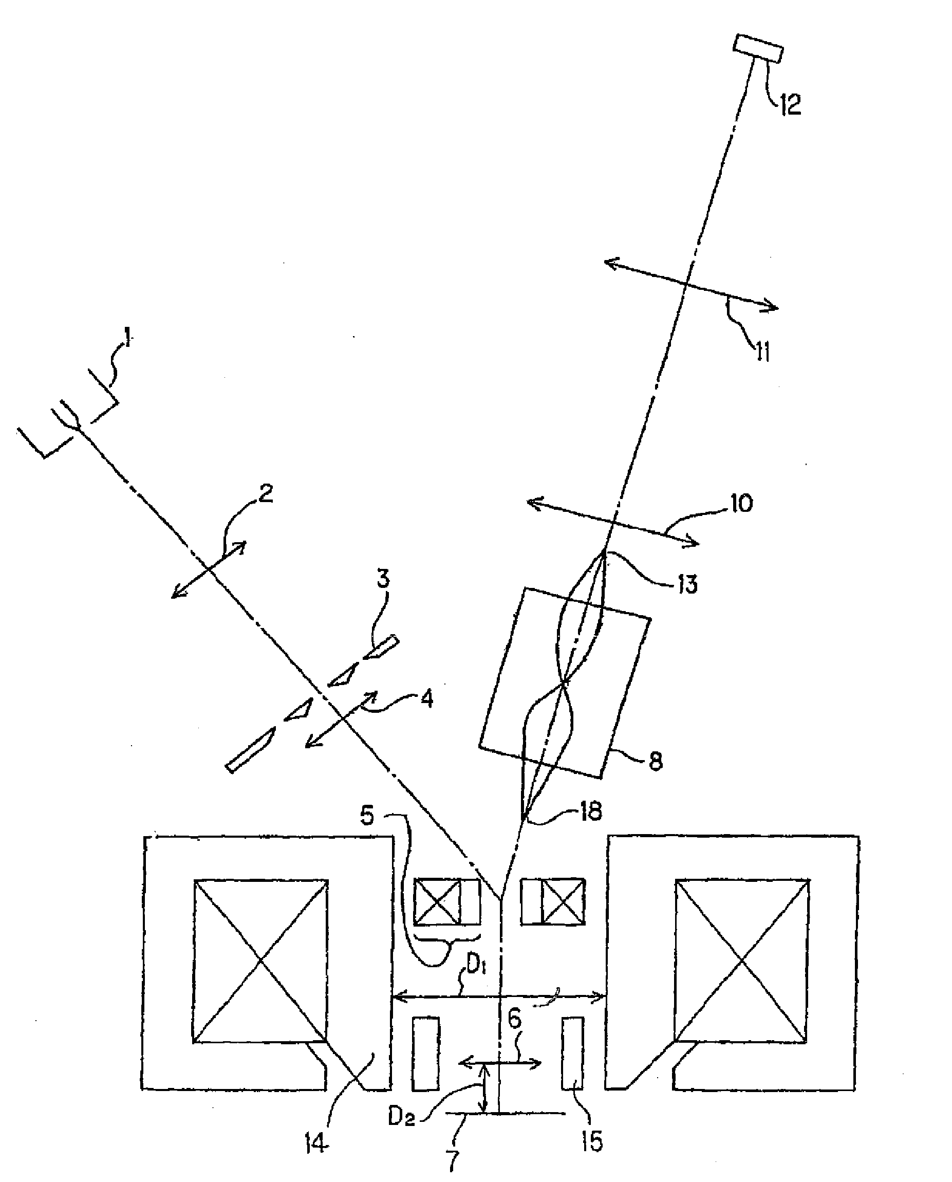
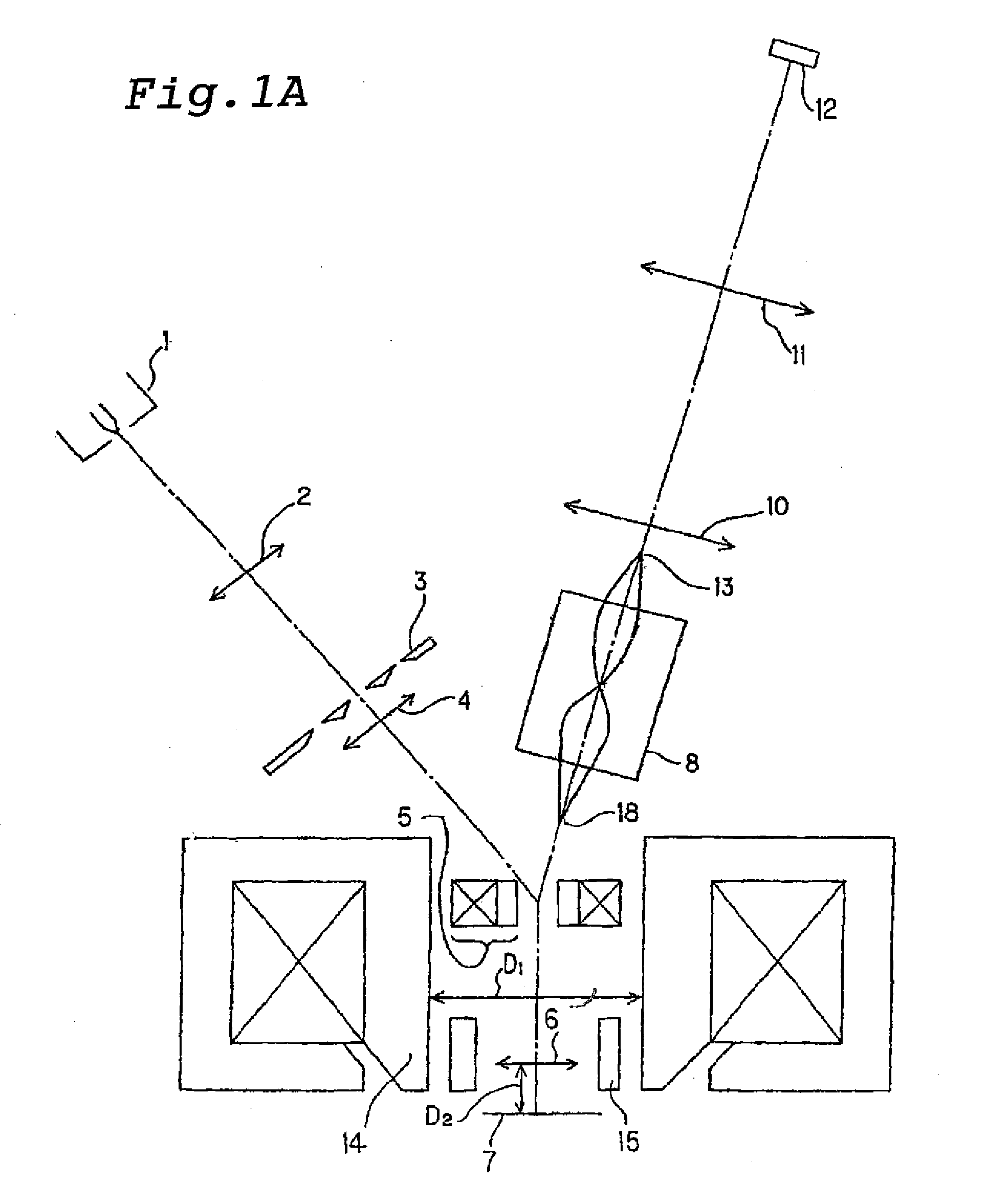
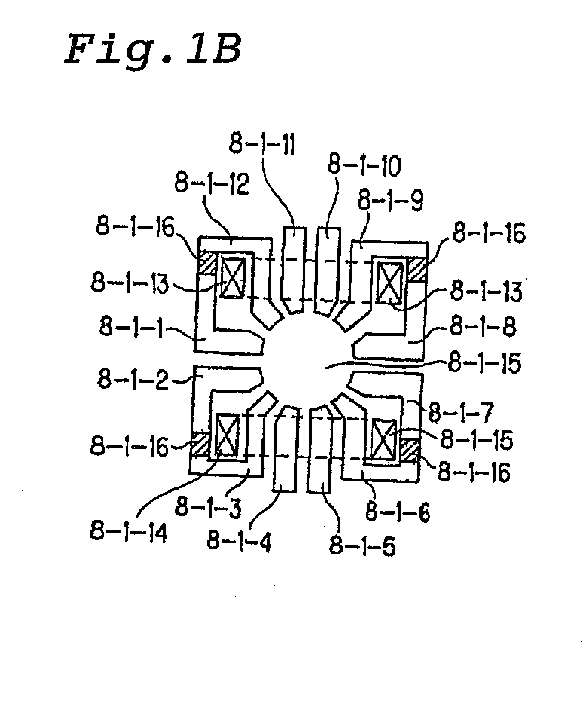
A sample is evaluated at a high throughput by reducing axial chromatic aberration and increasing the transmittance of secondary electrons. Electron beams emitted from an electron gun 1 are irradiated onto a sample 7 through a primary electro-optical system, and electrons consequently emitted from the sample are detected by a detector 12 through a secondary electro-optical system. A Wien filter 8 comprising a multi-pole lens for correcting axial chromatic aberration is disposed between a magnification lens 10 in the secondary electro-optical system and a beam separator 5 for separating a primary electron beam and a secondary electron beam, for correcting axial chromatic aberration caused by an objective lens 14 which comprises an electromagnetic lens having a magnetic gap defined on a sample side.

Description

TECHNICAL FIELD[0001]The present invention relates to a projection electron beam apparatus and a defect inspection system using the apparatus, and more particularly, to an electron beam apparatus which has a projection electro-optical system to have the abilities to conduct a defect inspection and the like for semiconductor wafer and the like at a high throughput, and a defect inspection apparatus using the apparatus. For example, the present invention relates to an electron beam apparatus which evaluates a sample having a pattern with a minimum line width of 0.25 μm or less and preferably 0.20 μm or less at high accuracy and high throughput, and a device manufacturing method using the apparatus.BACKGROUND ART[0002]Generally, in an electron beam apparatus which is configured to irradiate a sample applied with a retarding voltage with a primary electron beam and detect secondary electrons emitted from an irradiated spot to produce an image of the sample, a larger electric field must ...

Claims


Application Information

Patent Timeline
Patent Type & Authority Applications(United States)
IPC IPC(8): G01N23/00A61N5/00H01J1/50
CPCG01N23/2251H01J2237/057H01J37/28H01J37/05
Inventor NAKASUJI, MAMORUNOJI, NOBUHARUSATAKE, TOHRUMURAKAMI, TAKESHISOBUKAWA, HIROSIKAGA, TORU
Owner KK TOSHIBA
Learn More