Probe of vertical probe card

Inactive Publication Date: 2009-08-27
IPWORKS TECH CORP
View PDF3 Cites 8 Cited by
  • Summary
  • Abstract
  • Description
  • Claims
  • Application Information

AI Technical Summary

Benefits of technology

[0012]The present invention is related to a probe of a vertical probe card, which is applied a nano-film of electro-conductive nano-material to a surface region of the probe. Thus, according to of the present invention, the nano-film of the probe can efficiently provide better no-clean property, higher electro-conductivity, lower contact force, and longer usage lifetime for the probe of vertical probe card.
[0013]The present invention is related to a pr

Problems solved by technology

Thus, a wafer probing test is one of important processes in the integrated circuit fabrication, which affects the manufacture cost thereof.
Especially, a device requested for high electrical current testing, it may cause the probes tip are burned out.
As for device requested high temperature testing such as 75° C. or even 105° C., it may cause the die pad softened and easily wetted the probe tip.
As a result, lowering the electro-conductivity of the probe, increasing the resistance of the probe, and affecting the test reliability and lifetime of the probe card.
However, for the vertical probe card, because the probe tip of the probe may be wetted with foreign matter (such as solder from the pad), the test quality may be lowered or the mis-test probability may be increased, resulting in unexpectedly lowering the test yield.
Nev

Method used


Image

  • Probe of vertical probe card
  • Probe of vertical probe card

Examples


Embodiment Construction

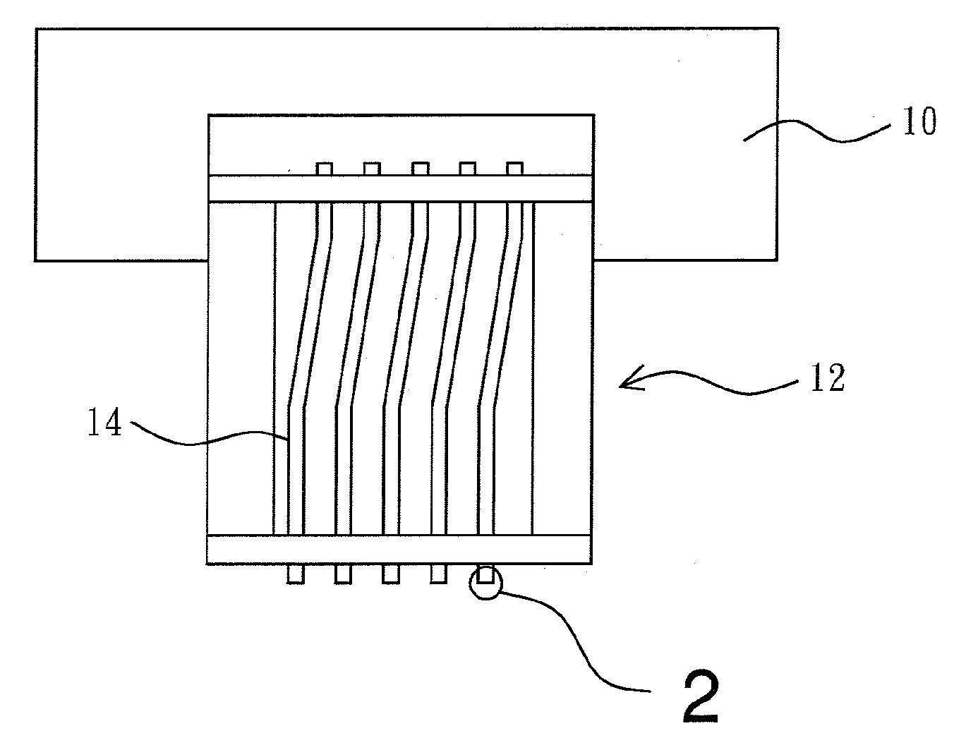
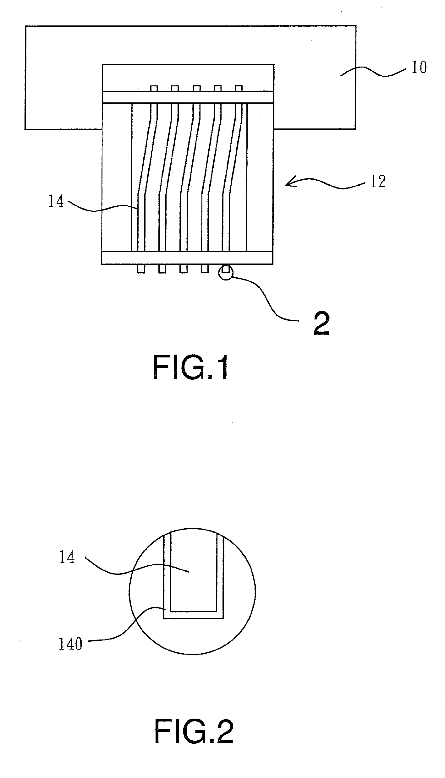
[0017]The present invention provides a probe of a vertical probe card, wherein the vertical probe card comprises a plurality of probes (or at least one probe) and a nano-film of electro-conductive nano-material. The probes are mounted on the vertical probe card and made of a metal material, while the nano-film of electro-conductive nano-material is coated on each of the probes.

[0018]In the present invention, the vertical probe card can be preferably selected from a micro-electromechanical system (MEMS) micro-array probe card manufactured by a MEMS process or a vertical pin probe card.

[0019]In the present invention, the nano-film of electro-conductive nano-material can be preferably selected from electro-conductive macromolecular having a no-clean property. For example, the electro-conductive nano-material can be selected from the group consisting of polypyrrole, polyparaphenylene, polythiophene, polyaniline, combination thereof, and derivative thereof. The thickness of the nano-film...


PUM


Abstract

A probe of a vertical probe card is disclosed. The probe has a probe tip and a surface region extended from the probe tip about 1-10 mil. The surface region is coated with a nano-film of high electro-conductive nano-material, and the thickness of the nano-film is about 1-20 nm. The nano-film of the probe can efficiently provide excellent no-clean property and higher electro-conductivity for lowering contact force and elongating usage lifetime of the probe of vertical probe card. Accordingly the yield of wafer testing can be improved, the frequency of cleaning probe can be lowered, and the total testing cost can be reduced.

Description

FIELD OF THE INVENTION[0001]The present invention relates to a probe of a probe card for a wafer probing test, and more particularly to a probe of a vertical probe card having a nano-film of electro-conductive nano-material on the probe.BACKGROUND OF THE INVENTION[0002]A probe card is constructed by a multi-layer printed circuit board (PCB) which may include more than 30 layers. The probe card has complicated structure and provides a plurality of probes for being in contact with a plurality of electrical contacts (i.e. pads) on a wafer, respectively. Generally, a contact area between each of the probes and each of the electrical contacts of the wafer is smaller than a cross-sectional area of a hair. Before an integrated circuit (IC) die is packaged by encapsulant, the probe card can be used to test electrical functions of the IC die cut from a wafer, in order to remove defective dies and keep known good dies for the following packaging processes. Thus, a wafer probing test is one of...

Claims


Application Information

Patent Timeline
IPC IPC(8): G01R1/067
CPCG01R3/00G01R1/06755
Inventor CHEN, BEEN-LONGCHEN, HUANG-CHIH
Owner IPWORKS TECH CORP
Why Eureka
Try Eureka