Tungsten liner for aluminum-based electromigration resistant interconnect structure

a technology of aluminum-based electromigration resistance and interconnect structure, which is applied in the direction of semiconductor devices, semiconductor/solid-state device details, electrical apparatus, etc., can solve the problems of metal line or metal via no longer providing a conductive path in the metal interconnect, metal ions to dislodge from the lattice and move physically, and product failure of semiconductor devices, etc., to achieve the effect of enhancing electromigration resistan

Inactive Publication Date: 2009-09-17
GLOBALFOUNDRIES INC
View PDF4 Cites 20 Cited by
  • Summary
  • Abstract
  • Description
  • Claims
  • Application Information

AI Technical Summary

Benefits of technology

[0017]According to the present invention, an underlying interconnect level containing underlying W vias embedded in a dielectric material layer are formed on a semiconductor substrate. A metallic layer stack comprising, from bottom to top, a low-oxygen-reactivity metal layer, a bottom transition metal layer, a bottom transition metal nitride layer, an aluminum-copper layer, an optional top transition metal layer, and a top transition metal nitride layer. The metallic layer stack is lithographically patterned to form at least one aluminum-based metal line, which constitutes a metal interconnect structure. The low-oxygen-reactivity metal layer enhances electromigration resistance of the at least one aluminum-based metal line since formation of compound between the bottom transition metal layer and the dielectric material layer is prevented by the low-oxygen-reactivity metal layer, which does not interact with the dielectric material layer.

Problems solved by technology

High defect density, i.e., smaller grain size of the metal, or high temperature typically increases electron scattering, and consequently, the amount of momentum transfer from the electrons to the conductor material.
Such momentum transfer, if performed sufficiently cumulatively, may cause the metal ions to dislodge from the lattice and move physically.
Such a void results in a locally increased resistance in the metal interconnect, or even an outright circuit “open.” In this case, the metal line or the metal via no longer provides a conductive path in the metal interconnect.
Formation of voids in the metal line or the metal via can thus result in a product failure in semiconductor devices.
On one hand, if the bottom Ti layer 920 becomes too thin, the sheet resistance of the bottom Ti layer 920 increases too much, which leads to earlier electromigration failure to a predetermined resistance level, as well as earlier failure by open circuit.
This reduces the volume of the material in the aluminum-copper layer 940 that is required to be removed by electromigration to form a void, thus rendering the second prior art aluminum-based metal wire structure more prone to electromigration and shortening the electromigration life.
This has the effect of producing a noticeable resistance shift due to electromigration in a shorter time than if the entire volume of AlCu alloy is removed, prompting earlier electromigration failures in the second prior art aluminum-based metal wire structure.
A consequence of such various electromigration effects is that a series of small process changes over several years can degrade the electromigration performance of the metallization.
Statistically, when sufficient quantity of hardware is subjected to electromigration stress, frequency of early failure increases and the usable current density of the metallization degrades.
Variations in the thickness of bottom Ti layer 920 and anneal conditions have been attempted to improve the performance in anneal metallurgy structures such as the first prior art aluminum-based metal wire structure, such an approach induces performance tradeoffs (e.g., resistance per unit) that result in poor yields as dimensions of metallization structures shrink.
In addition, lithographic requirements of deep-ultraviolet (DUV) technology often necessitate the use of dielectric ARC layers, which impart stresses on the anneal metallurgy structures such that materials extrude when heated and may induce electrical shorts.
However, such design modifications compromise the designs in areal circuit density and cost.

Method used


Image

  • Tungsten liner for aluminum-based electromigration resistant interconnect structure
  • Tungsten liner for aluminum-based electromigration resistant interconnect structure
  • Tungsten liner for aluminum-based electromigration resistant interconnect structure

Examples


first embodiment

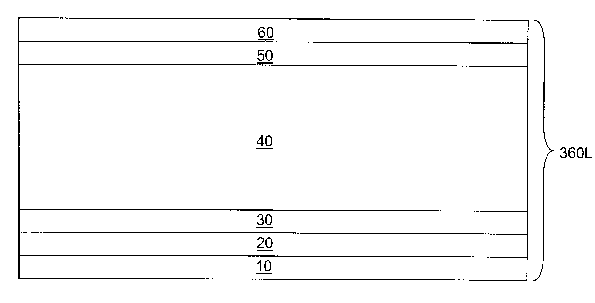
[0051]Four embodiments are provided for the structure of the metallic stack 360L according to the present invention. Referring to FIG. 5, a first exemplary structure for the metallic stack 360L is shown according to the present invention. The first exemplary structure for the metallic stack 360L comprises, from bottom to top, a low-oxygen-reactivity metal layer 10, a bottom transition metal layer 20, a transition metal nitride layer 30, an aluminum-copper layer 40, a top transition metal layer 50, and a top transition metal nitride layer 60. The bottom transition metal layer 20 is formed directly on the low-oxygen-reactivity metal layer 10, and vertically abuts the low-oxygen-reactivity metal layer 10. The bottom transition metal nitride layer 30 is formed directly on the bottom transition metal layer 20, and vertically abuts the bottom transition metal layer 20. The aluminum-copper layer 40 is formed directly on the bottom transition metal nitride layer 30, and vertically abuts the...

second embodiment

[0068]Referring to FIG. 6, a second exemplary structure for the metallic stack 360L is shown according to the present invention. The second exemplary structure for the metallic stack 360L may be incorporated into the exemplary metal interconnect structure of FIG. 4 instead of the first exemplary structure for the metallic stack 360L. The second exemplary structure for the metallic stack 360L comprises, from bottom to top, a low-oxygen-reactivity metal layer 10, a bottom transition metal layer 20, a transition metal nitride layer 30, an aluminum-copper layer 40, and a top transition metal nitride layer 60.

[0069]The structure, composition, and method of manufacture of each of the layers comprising the second exemplary structure for the metallic stack 360L are the same as in the first embodiment. Specifically, the second exemplary structure for the metallic stack 360L according to the second embodiment of the present invention may be derived from the first exemplary structure for the m...

third embodiment

[0070]Referring to FIG. 7, a third exemplary structure for the metallic stack 360L is shown according to the present invention. The third exemplary structure for the metallic stack 360L may be incorporated into the exemplary metal interconnect structure of FIG. 4 instead of the first exemplary structure for the metallic stack 360L. The second exemplary structure for the metallic stack 360L comprises, from bottom to top, a bottommost transition metal nitride layer 8, a low-oxygen-reactivity metal layer 10′, a bottom transition metal layer 20, a transition metal nitride layer 30, an aluminum-copper layer 40, a top transition metal layer 50, and a top transition metal nitride layer 60.

[0071]The structure, composition, and method of manufacture of each of the bottom transition metal layer 20, the transition metal nitride layer 30, the aluminum-copper layer 40, and the top transition metal nitride layer 60 are the same as in the first embodiment. Specifically, the third exemplary structu...


PUM

PropertyMeasurementUnit
thicknessaaaaaaaaaa
dielectric constantaaaaaaaaaa

Abstract

An underlying interconnect level containing underlying W vias embedded in a dielectric material layer are formed on a semiconductor substrate. A metallic layer stack comprising, from bottom to top, a low-oxygen-reactivity metal layer, a bottom transition metal layer, a bottom transition metal nitride layer, an aluminum-copper layer, an optional top transition metal layer, and a top transition metal nitride layer. The metallic layer stack is lithographically patterned to form at least one aluminum-based metal line, which constitutes a metal interconnect structure. The low-oxygen-reactivity metal layer enhances electromigration resistance of the at least one aluminum-based metal line since formation of compound between the bottom transition metal layer and the dielectric material layer is prevented by the low-oxygen-reactivity metal layer, which does not interact with the dielectric material layer.

Description

FIELD OF THE INVENTION [0001]The present invention relates to semiconductor structures, and particularly to aluminum-based electromigration resistant metal interconnect structures employing a low-oxygen-reactivity metal layer as a barrier layer, and methods of manufacturing the same.BACKGROUND OF THE INVENTION [0002]A metal line comprises a lattice of metal ions and non-localized free electrons. The metal ions are formed from metal atoms that donate some of their electrons to a common conduction band of the lattice, and the non-localized free electrons move with relatively small resistance within the lattice under an electric field. Normal metal lines, excluding superconducting materials at or below a superconducting temperature, have finite conductivity, which is caused by interaction of electrons with crystalline imperfections and phonons which are thermally induced lattice vibrations.[0003]When electrical current flows in the metal line, the metal ions are subjected to an electro...

Claims


Application Information

Patent Timeline
Patent Type & Authority Applications(United States)
IPC IPC(8): H01L23/532H01L21/768
CPCH01L23/53223H01L23/5329H01L2221/1078H01L2924/0002H01L2924/00
Inventor CHAPPLE-SOKOL, JONATHAN D.DELIBAC, DANIEL A.HE, ZHONG-XIANGLEE, TOM C.MURPHY, WILLIAM J.SULLIVAN, TIMOTHY D.THOMAS, DAVID C.VANSLETTE, DANIEL S.
Owner GLOBALFOUNDRIES INC
Why Eureka
Try Eureka