

Photoelectric conversion element
- Summary
- Abstract
- Description
- Claims
- Application Information
AI Technical Summary
Benefits of technology
Problems solved by technology
Method used
Image

Examples
first embodiment
[0114]An example of the photoelectric conversion element of the present invention will be described in accordance with FIGS. 1 through 12.
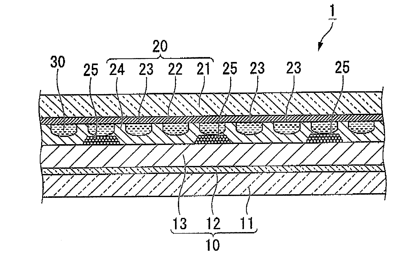
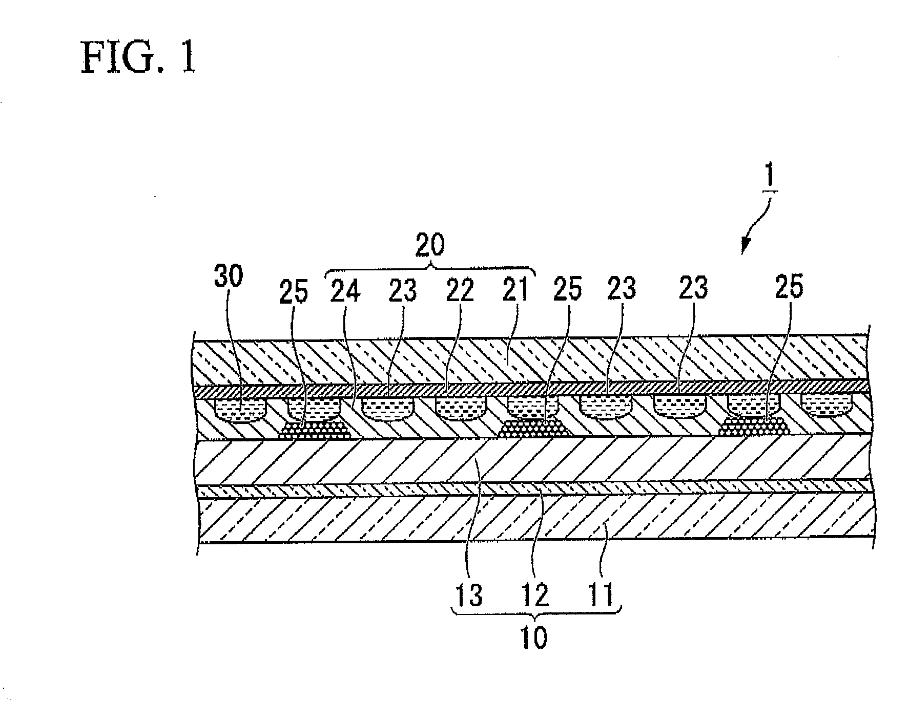
[0115]FIG. 1 is a sectional view illustrating an example (a first structure) of a photoelectric conversion element according to the present invention.
[0116]As shown in FIG. 1, the photoelectric conversion element 1 according to the present embodiment includes a first electrode 10 having a porous oxide semiconductor layer 13 which supports a sensitizing dye on a surface of it, and functioning as a photo electrode, a second electrode 20 disposed so as to oppose the first electrode 10, and an electrolyte 30 disposed at least in a part of a space between the two electrodes. Further, the photoelectric conversion element 1 is structured with sump portions 23 which are composed respectively of a recessed portion and are provided in predetermined positions of a conductive porous portion 24.
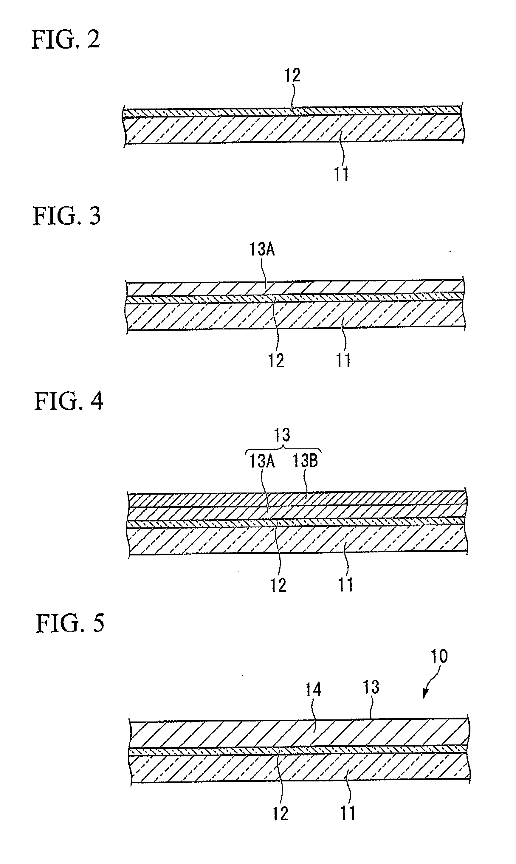
[0117]The first electrode 10 is prepared by forming an FTO conduct...
second embodiment
[0156]Next, another example of the photoelectric conversion element of the present invention will be described in accordance with FIGS. 13 through 16.
[0157]FIG. 13 is a schematic sectional view illustrating another example (a second structure) of a photoelectric conversion element according to the present invention.
[0158]As shown in FIG. 13, a photoelectric conversion element (or a wet type solar cell) 41 according to the present embodiment includes a first electrode 10 having a porous oxide semiconductor layer (also referred to as “oxide electrode”) 13 which supports a sensitizing dye on a surface of it, and functioning as a photo electrode (also referred to as “working electrode”), a second electrode 50 disposed so as to oppose the first electrode 10, and an electrolyte 30 disposed at least in a part of the space between the two electrodes. Further, the photoelectric conversion element 41 is structured with sump portions 53 which are composed respectively of a void space formed be...
third embodiment
[0176]Next, still another example of the photoelectric conversion element of the present invention will be described in accordance with FIGS. 17 through 21.
[0177]FIG. 17 is a schematic sectional view illustrating another example (a third structure) of a photoelectric conversion element according to the present invention.
[0178]As shown in FIG. 17, a photoelectric conversion element (or a wet type solar cell) 61 according to the present embodiment includes a first electrode 10 having a porous oxide semiconductor layer (also referred to as “oxide electrode”) 13 which supports a sensitizing dye on a surface of it, and Rationing as a photo electrode (also referred to as “working electrode”), a second electrode 70 disposed so as to oppose the first electrode 10, and an electrolyte 30 disposed in at least a part of the space between the two electrodes. Further, the photoelectric conversion element 61 is structured in a manner in which sump portions 73 composed respectively of a recessed po...
PUM
 Abstract
Description
Claims
Application Information