Display Substrate Having a Transparent Conductive Layer Made of Zinc Oxide and Manufacturing Method Thereof

a technology of zinc oxide and conductive layer, which is applied in the direction of conductive layer on the insulating support, identification means, instruments, etc., can solve the problems of low resistance, inability to use, and indium (in), an element constituting the ito film, etc., and achieve high transmission rate, low resistance, and high adhesion.

Inactive Publication Date: 2009-10-01
CASIO COMPUTER CO LTD +1
View PDF8 Cites 23 Cited by
  • Summary
  • Abstract
  • Description
  • Claims
  • Application Information

AI Technical Summary

Benefits of technology

[0025]It is to be understood that the present invention provides a display substrate comprising a transparent conductive film, which provides a high adhesion to a resin-coated substrate, a high transmission rate in the visible light range, a low resistance, and neat appearance thanks to its simple structure, a manufacturing method thereof, and a display device adopting the display substrate. The present invention is applicable not only to color filters but also to transparent ZnO electrodes on other resin substrates.

Problems solved by technology

However, since ITO films turn black in oxygen plasma due to reduction, they cannot be used as electrodes in a process in which amorphous silicon is deposited by chemical vapor deposition, following a ZnO deposition process, as in the case of solar battery manufacturing process.
Furthermore, indium (In), an element constituting the ITO film, is expensive and scarce rare metal.
On the other hand, fluorin-doped SnO2:F films whose resistivity is as high as 10−3 Ω·cm are not suitable for films required to provide high conductivity.
To minimize the reduction of transmittance, the Ag film 3 must be formed thin, but this control is unfeasible.
In addition, a major element of the ITO film 11 used as the uppermost layer is indium (In), which is a rare metal and therefore expensive.
Furthermore, this prior literature does not give any consideration to the fluctuation of sheet resistance of the ZnO film that occurs when the color filter layer is subjected to heat treatment.
The use of Ag and ITO, in addition to ZnO, in the transparent conductive film in the previous literature thus causes various problems.

Method used


Image

  • Display Substrate Having a Transparent Conductive Layer Made of Zinc Oxide and Manufacturing Method Thereof
  • Display Substrate Having a Transparent Conductive Layer Made of Zinc Oxide and Manufacturing Method Thereof
  • Display Substrate Having a Transparent Conductive Layer Made of Zinc Oxide and Manufacturing Method Thereof

Examples


example 1

[0097]Hereinafter, an example of the present invention will be described in more detail.

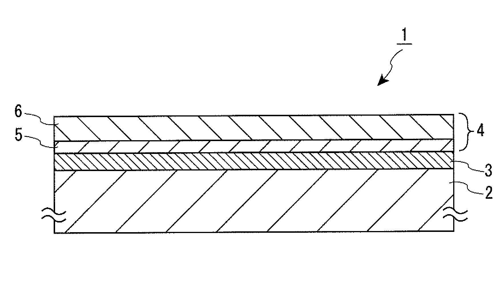
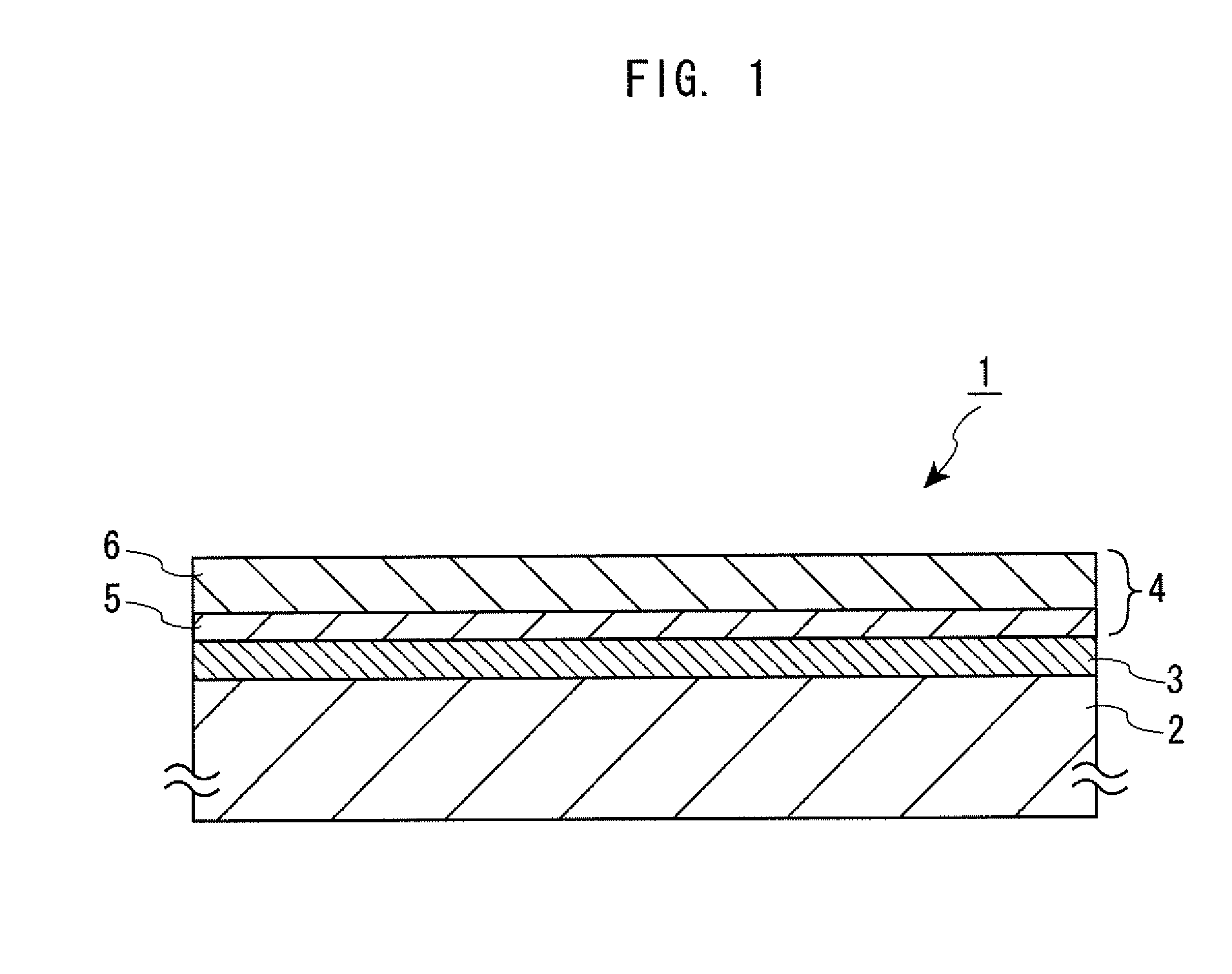
[0098]A commercially available substrate having color filter layers (organic resin layer) 3 is prepared. The transparent electrode film 4 made of GZO was deposited by sputtering onto the color filter layer 3. The used supporting substrate 2 was the glass substrate containing no alkaline. For an example, this supporting substrate is #1737 made by the Corning Incorporated. A size of the glass supporting substrate 2 was 320 mm×440 mm. The sputtering equipment changeable between the DC sputtering mode and the DC / RF sputtering mode, in which DC radio frequency power is superimposed upon the DC sputtering, was used. The ratio of DC power to RF power was set to 1:1 in the DC / RF mode, and the frequency of RF power was set to 13.56 MHz.

[0099]The display substrate 1 in Example 1 was manufactured by depositing a GZO film, which serves as the first layer 5, onto the color filter layers 3 formed on the suppor...

example 2

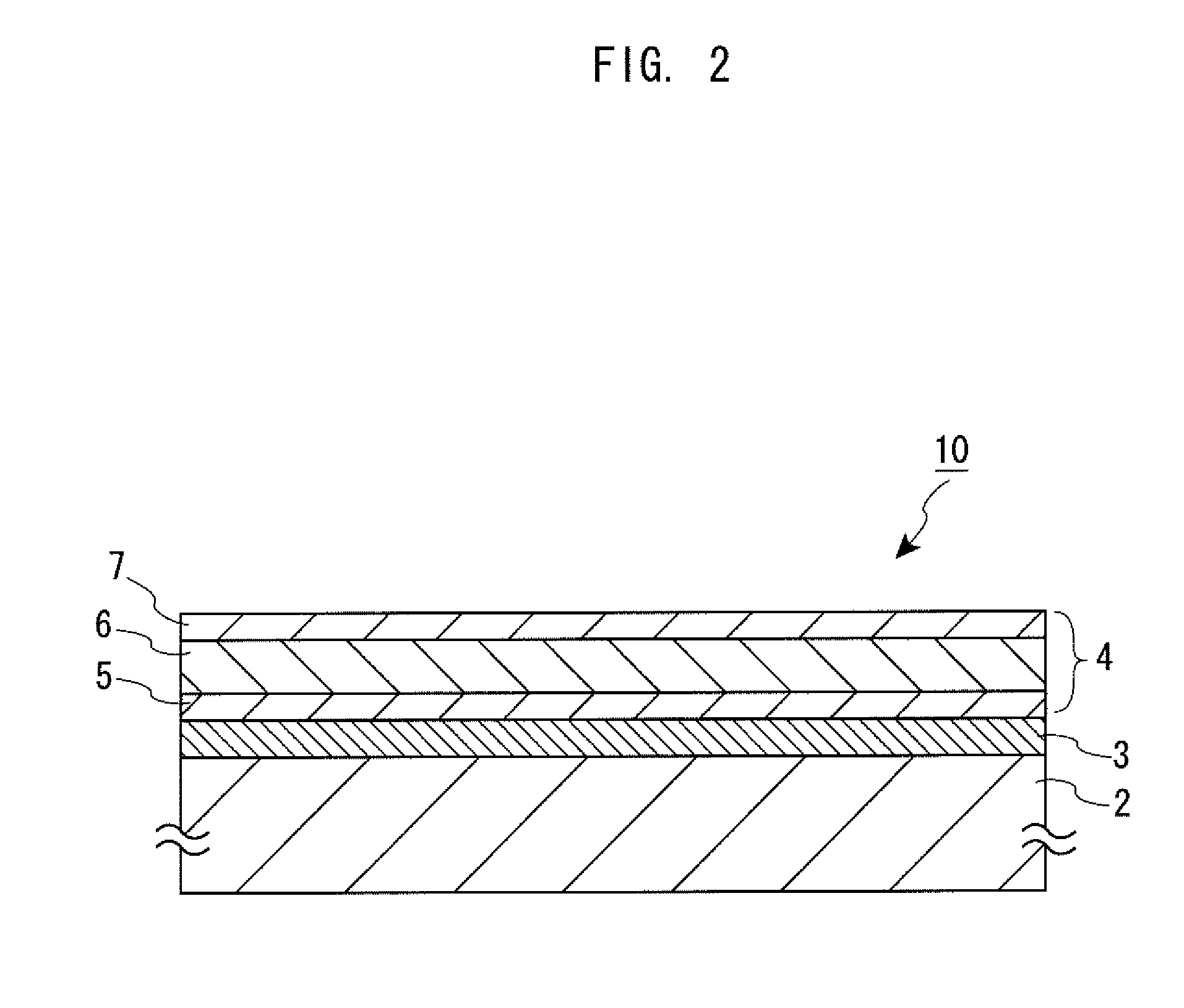
[0100]The display substrate 10 in Example 2 was manufactured by depositing GZO film, which serves as the first layer 5, onto the color filter layer 3 formed on the same glass supporting substrate 2 as Example 1 in thickness of 20 nm in the DC sputtering mode. The GZO film was then deposited as the second layer 6 in thickness of 110 nm in the DC / RF sputtering mode, and then the GZO film as the third layer 7 in thickness of 20 nm in the DC sputtering mode. The conditions other than this deposition condition were the same manner as that of Example 1.

example 3

[0101]The display substrate 10 in Example 3 was manufactured by depositing the buffer layer 3b first in thickness of 20 nm onto the color filter layer 3a formed onto the same glass supporting substrate 2 in Example 1, the GZO film was then deposited as the first layer 5 in the DC sputtering mode in thickness of 20 nm, the GZO film as the second layer 6 in the DC / RF sputtering mode in thickness of 110 nm, and lastly the GZO film as the third layer 7 in the DC sputtering mode in thickness of 20 nm.


PUM

PropertyMeasurementUnit
resistivityaaaaaaaaaa

Abstract

A display substrate is disclosed comprising: a supporting substrate; an organic resin layer formed on the supporting substrate; and a transparent electrode formed on the organic resin layer, wherein the transparent electrode includes: a first layer containing a zinc oxide and formed in close contact with the organic resin layer; and a second layer containing a zinc oxide and which has a thickness thicker than a thickness of the first layer and is formed on the first layer, wherein the first layer is deposited by either one of a DC sputtering and a DC magnetron sputtering, and the second layer is deposited by any one of a radio frequency sputtering, a radio frequency magnetron sputtering, a radio frequency superimposing a DC sputtering, and a radio frequency superimposing a DC magnetron sputtering, and the display substrate is available, for example, as the substrate having a transparent electrode for counter electrode of liquid crystal display device.

Description

[0001]This application is based upon and claims the benefit of Japanese Patent Application No. 2008-094411, filed in Japan on Mar. 31, 2008, and Japanese Patent Application No. 2009-055755, filed in Japan on Mar. 9, 2009, both of which are hereby incorporated by reference in their entries.BACKGROUND OF THE INVENTION[0002]1. Field of the Invention[0003]The present invention relates to a display substrate comprising a transparent conductive layer, which uses deposited zinc oxide as a base material and provides a high transmission rate in the visible light range, a high conductivity, and a high adhesiveness to a resin substrate, and a manufacturing method thereof.[0004]2. Description of the Related Art[0005]As transparent electrodes for devices in display devices such as liquid crystal and plasma displays, thin-film solar batteries, input devices such as touch panels, and electronic devices such as light-emitting diodes, indium tin oxide (ITO), fluorin-doped tin oxide (SnO2: F), boron-...

Claims


Application Information

Patent Timeline
Patent Type & Authority Applications(United States)
IPC IPC(8): H01L33/00H01L21/28C23C14/32C23C14/08G02F1/1333G02F1/1335G02F1/1343G09F9/30H01B5/14
CPCC23C14/086C23C14/34H01L51/5206G02F1/13439C23C14/3485H10K59/80517H10K50/816
Inventor YAMAMOTO, TETSUYAYAMAMOTO, NAOKIMAKINO, HISAOUJIHARA, AKIRAHIRASHIMA, YOSHINORIIWAOKA, HIROAKIAOKI, HISASHIHOKARI, HITOSHIYOSHIDA, MOTOHIKO
Owner CASIO COMPUTER CO LTD
Why Eureka
Try Eureka