Surface Acoustic Wave Element and Communication Device

a surface acoustic wave and communication device technology, applied in piezoelectric/electrostrictive/magnetostrictive devices, piezoelectric/electrostriction/magnetostriction machines, electrical apparatus, etc., can solve the problems of low power handling capability to be used as duplexers, inability to achieve sufficient characteristics, and damage to electrodes, etc., to achieve improved power handling capability of electrode fingers, improved power handling capability, and improved power handling capability

Active Publication Date: 2009-10-01
KYOCERA CORP
View PDF14 Cites 24 Cited by
  • Summary
  • Abstract
  • Description
  • Claims
  • Application Information

AI Technical Summary

Benefits of technology

[0037]In comparison to this, the surface acoustic wave element with this structure includes an IDT electrode comprising metal layers is formed on a piezoelectric substrate, the metal layers include crystal grains that are continuously formed to extend from a surface distant from the surface of the piezoelectric substrate to a surface close to the piezoelectric substrate, by which crystal grain boundaries where dangling bonds are present are not allowed to exist in larger amount on a principal surface in parallel to the piezoelectric substrate than in the film thickness direction. This reduces the density of crystal grain boundaries, and regions where hillocks are prone to generate. As a result, the power handling capability of the electrode fingers can be improved, so that a surface acoustic wave element having higher power handling capability can be realized.
[0038]It is preferred ...

Problems solved by technology

However, since dielectric duplexers cannot be miniaturized in principle in the frequency range in the present communication standards, and the attenuation characteristic in the vicinity of the passband cannot be made steep, it has been impossible to achieve sufficient characteristics in the communication standards where the transmitting frequency band and the receiving frequency band are close in the vicinity.
While surface acoustic wave elements have been used as interstage filters, they have low power handling capability to be used as duplexers.
For this reason, since a great deal of stress is applied at a high frequency to the electrode, atoms of the material constituting the el...

Method used


Image

  • Surface Acoustic Wave Element and Communication Device
  • Surface Acoustic Wave Element and Communication Device
  • Surface Acoustic Wave Element and Communication Device

Examples


example 1

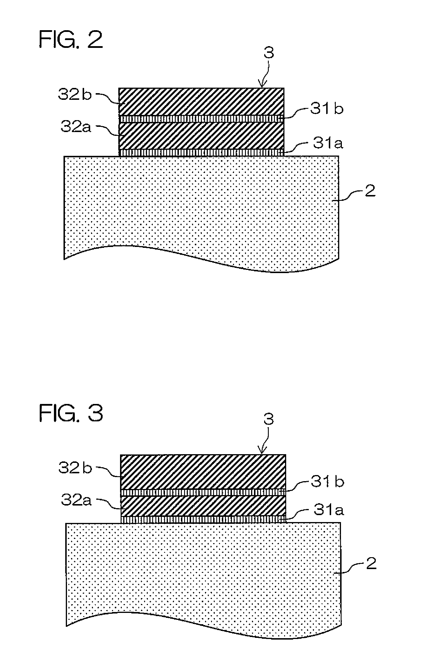
[0168]On a principal surface of a piezoelectric substrate 2 (with a thickness of 250 μm) comprising a 38.7° rotated, Y-cut, X-propagation single crystalline lithium tantalite, four conductive layers were formed including, in the order from the substrate side, Ti (first metal layer 31a) / Al and 1% by mass orientation degrees of the first metal layer 31a and the second metal layer 32a were higher than those of the first metal layer 31b and the second metal layer 32b as later described.

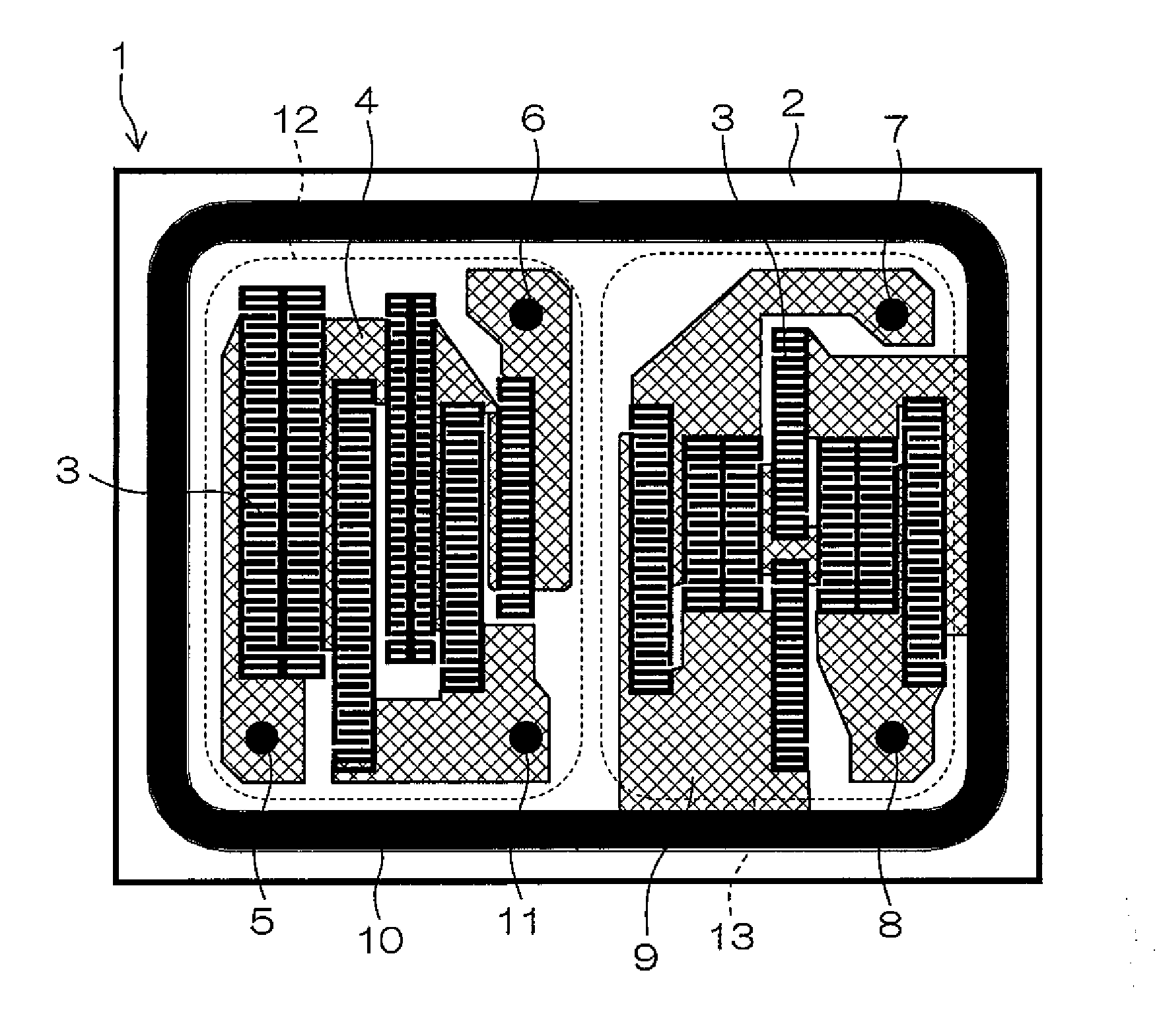
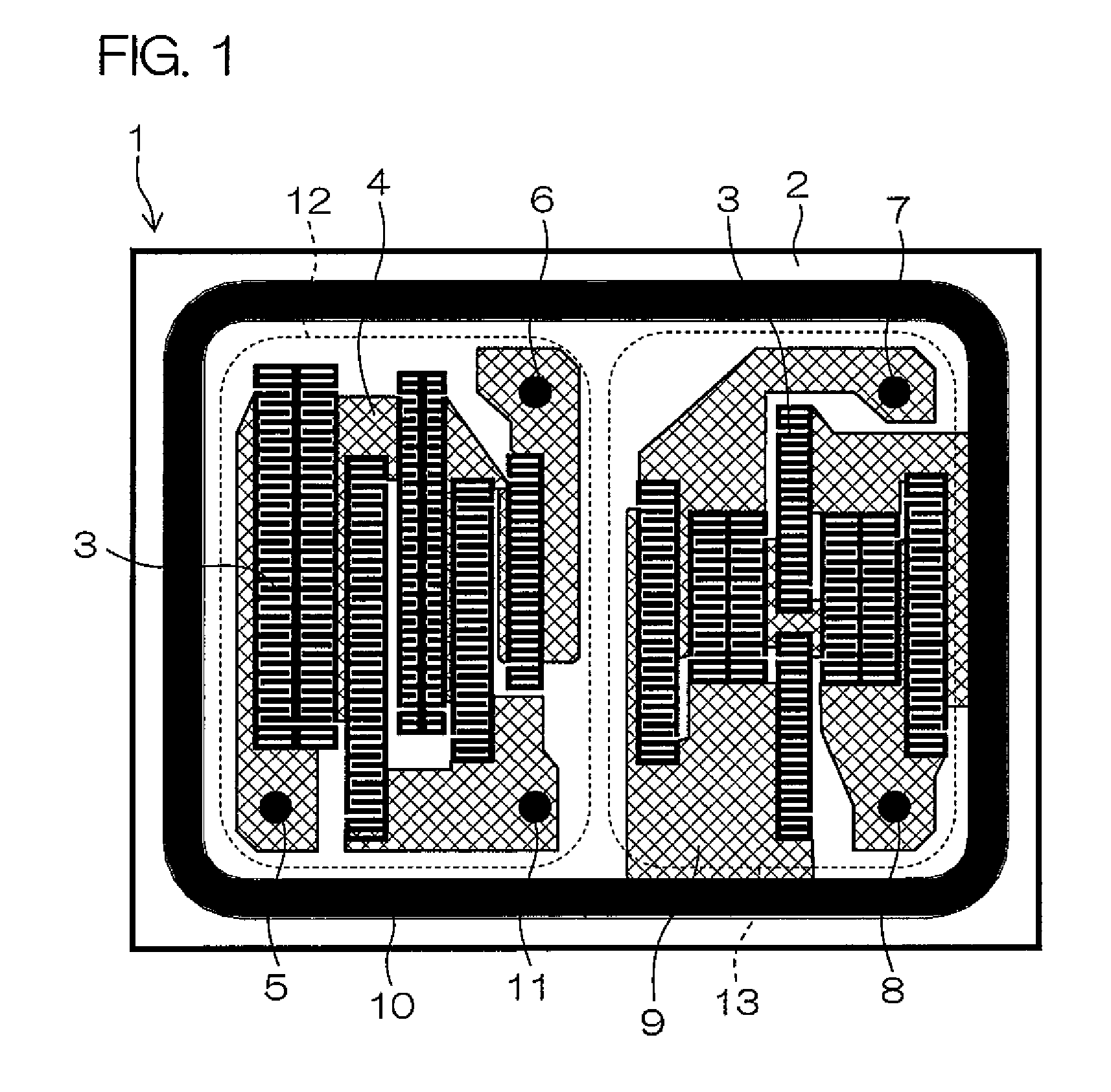
[0169]Subsequently, these conductive layers were subjected to patterning by photolithography and RIE so as to form a large number of surface acoustic wave element areas, each including a transmitting side filter area 12 and a receiving side filter area 13 that have IDT electrodes 3, input pad sections 5, 7 and output pad sections 6, 8 and a circumferential electrode 10 as shown in FIG. 1. The etching gas used herein was a gas mixture of BCl3 and Cl2. The line widths of electrode fingers constituting the I...

example 2

[0177]On a principal surface of a piezoelectric substrate 2 (with a thickness of 25 μm) comprising 38.7° rotated, Y-cut, X-propagation single crystalline lithium tantalite, a metal layer composed of Al and 1% by mass of Cu by sputtering. The thickness of the layer was 390 nm. The forming was carried out with conditions optimized by increasing the plasma input power and the film forming rate from those in a conventional case so that each one of crystal grains continuously grows in the thickness direction of the metal layer from the upper surface to the lower surface.

[0178]The film forming conditions in the present example were as follows: Ar flow rate of 100 sccm; film forming pressure of 0.25 Pa; input power of 800 W during the forming of Ti layer; input power of 3 kW during the forming of Al—Cu layer. However, since the optimum values of the forming conditions largely depend on the apparatus and the use situations of the targets, these forming conditions are not invariant, but the ...


PUM


Abstract

An IDT electrode (3) on a piezoelectric substrate (2) has an electrode including first metal layers (31a, 31b) formed of titanium or a titanium alloy, or chromium or a chromium alloy and second metal layers (32a, 32b) formed of aluminum or an aluminum alloy, copper or a copper alloy, or gold or a gold alloy, which are laminated alternately. The orientation degrees in the first metal layer (31a) that is closest to the surface of the piezoelectric substrate (2) in the first metal layers (31a, 31b) and the second metal layer (32a) that is closest to the surface of the piezoelectric substrate (2) in the second metal layers (32a, 32b) are higher than the orientation degrees in the upper metal layers. As compared with the prior art where the orientation degrees in the first metal layers (31a, 31b) and the second metal layers (32a, 32b) are not considered, the power handling capability of the IDT electrode (3) can be significantly improved.

Description

TECHNICAL FIELD[0001]The present invention relates to a surface acoustic wave element and a communication device. More specifically, the present invention relates to a surface acoustic wave element used as a duplexer, in particular, to a surface acoustic wave element including an IDT electrode with improved power handling capability, and a communication device using the surface acoustic wave element.BACKGROUND ART[0002]Recently, surface-mounted components are required to be smaller and lighter in accordance with the recent multi-functioned communication devices.[0003]One of such surface-mounted components is a duplexer for separating signals into the signals in the transmitting frequency band and the signals in the receiving frequency band, and dielectrics have been employed for conventional duplexers. However, since dielectric duplexers cannot be miniaturized in principle in the frequency range in the present communication standards, and the attenuation characteristic in the vicini...

Claims


Application Information

Patent Timeline
IPC IPC(8): H01L41/047
CPCH03H9/14541
Inventor YOKOTA, YUUKONAGAMINE, SHIGEHIKOYAMAHARA, KIYO
Owner KYOCERA CORP
Why Eureka
Try Eureka