Flat magnetic element and power IC package using the same

a magnetic element and power ic technology, applied in the direction of magnetic bodies, magnetic/solid-state device details, other domestic objects, etc., can solve the problems of reducing the height affecting the realization of the low-loss and high-inductance device, and reducing the realization of the high-inductance device. achieve the effect of improving the magnetic permeability to the magnetic field, reducing the height, and improving the inductan

Active Publication Date: 2009-10-01
KK TOSHIBA +1
View PDF12 Cites 63 Cited by
  • Summary
  • Abstract
  • Description
  • Claims
  • Application Information

AI Technical Summary

Benefits of technology

[0035]The power source IC package according to the present invention is formed by mounting the planar magnetic device prepared as described above, a control IC and a semiconductor chip such as a field effect transistor (FET) on an identical substrate or an identical package in a planar direction or a height direction. Particularly, the feature of the power source IC package, i.e. the IC integrated type wherein the planar magnetic device and the IC chip are integrally mounted on one substrate, is effective for device downsizing. Also, it is possible to achieve the one-package by integrally mounting a plurality of semiconductor chips and an active device. For example, a power source function such as a DC-DC converter may be incorporated into the package, or a similar power source function is achieved by providing an external capacitor.
[0036]According to the planar magnetic device having the above-described structure, since the magnetic fine particles having the shape ratio S / L that is a ratio between the long axis length (L) and the length of the short axis (S) orthogonal to the long axis is 0.7 to 1 are filled in the gap between the wirings, it is possible to improve the magnetic permeability to the magnetic field generated on the planar coil, thereby realizing the magnetic device serving as an inductor improved in inductance and reduced in height.
[0037]Further, it is also possible to obtain the one-package by mounting the planar magnetic device prepared as described above, a control IC, and a semiconductor chip such as a field effect transistor (FET) on an identical substrate or an identical package in a planar direction or a height direction, thereby making it possible to achieve high density mounting of functional devices as well as to exhibit a prominent effect for achieving a small and high performance semiconductor device.

Problems solved by technology

The former one is increased in proportion of a surface deteriorated layer caused by process distortion due to polishing to a total volume along with downsizing and thinning of a bulk ferrite core, so that the characteristic such as a magnetic permeability are deteriorated to hamper realization of an inductor device achieving a low loss and high inductance.
However, among the above-described conventional inductors, the former one is increased in proportion of surface deteriorated layer caused by process distortion due to polishing to a total volume along with downsizing and thinning of a bulk ferrite core, so that the characteristic such as a magnetic permeability are deteriorated to hamper realization of high inductance device having a reduced height.
Also, since magnetic permeability of the latter one is generally low, the latter one has a drawback of having difficulty in achieving a large inductance value, and there has been a limit for the height reduction of a magnetic device such as the inductor when a large amount of magnetic material is used for compensating for the drawback.

Method used


Image

  • Flat magnetic element and power IC package using the same
  • Flat magnetic element and power IC package using the same
  • Flat magnetic element and power IC package using the same

Examples


example 1

[0047]Fine magnetic particles were prepared by treating a molten material of sendust having an alloy composition of 5.5 wt. % Al-10 wt. % Si—Fe by a water-gas atomizing method. Specifically, the magnetic particles were prepared by dispersing the molten material by injecting the molten material out from a furnace while simultaneously spraying an inert gas (Ar), and introducing the dispersed particles into water for rapid cooling.

[0048]The magnetic particles obtained as described above had an average diameter (50% by volume) of 28 μm, and only magnetic particles having the size less than 63 μm were selected by passing the magnetic particles through a sieve having a mesh opening of 63 μm. As a result, the magnetic particles having a shape ratio S / L and an average particle diameter D shown in Table 1 were prepared. Further, a paste was prepared by mixing 1.4 mass % of a vehicle (binder) with the magnetic particles.

[0049]Next, on an upper surface of a Si substrate having the thickness of...

example 2

[0060]Amorphous magnetic particles were obtained by dispersing a molten material having an alloy composition of (Co0.90-Fe0.05-Mn0.02-Nb0.03)71-Si15-B14 by an atomic ratio by injecting the molten material out from a furnace in accordance with a water atomization method and a gas atomization method while simultaneously spraying an inert gas (Ar) to the molten material and introducing the dispersed particles into water for rapid cooling.

[0061]The thus-obtained magnetic particles had an average diameter (50% by volume) of 14 μm, and only magnetic particles having the size less than 32 μm were selected by passing the magnetic particles through a sieve having a mesh opening of 32 μm. After that, a paste was prepared by mixing a vehicle (binder) of 0.9 mass % with the magnetic particles, and a patterned magnetic sheet having the thickness of 100 μm and the size of 10 mm×10 mm was printed on a Si substrate to form a first magnetic layer 3.

[0062]After forming the magnetic pattern (first mag...

examples 3 to 11

[0067]Magnetic particles having the shape ratio and the average particle diameter shown in Table 1 were prepared by pulverizing and sieving the sendust used in Example 2, the Co-based amorphous alloy used in Example 2, and a ferrite alloy having a composition of Ni0.5Zn0.5Fe2O4 (molar ratio). A magnetic material paste was prepared by mixing the thus-obtained magnetic particles with a binder in a predetermined amount that is the content shown in Table 1.

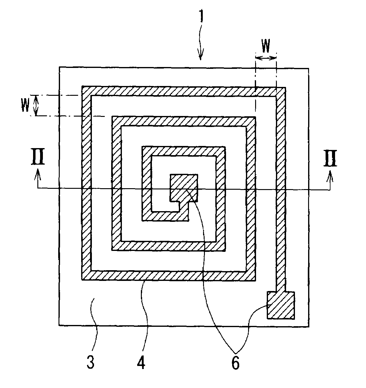
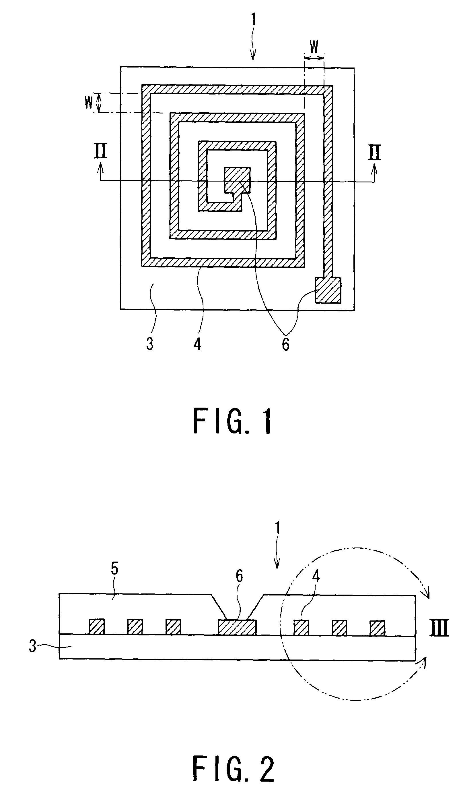
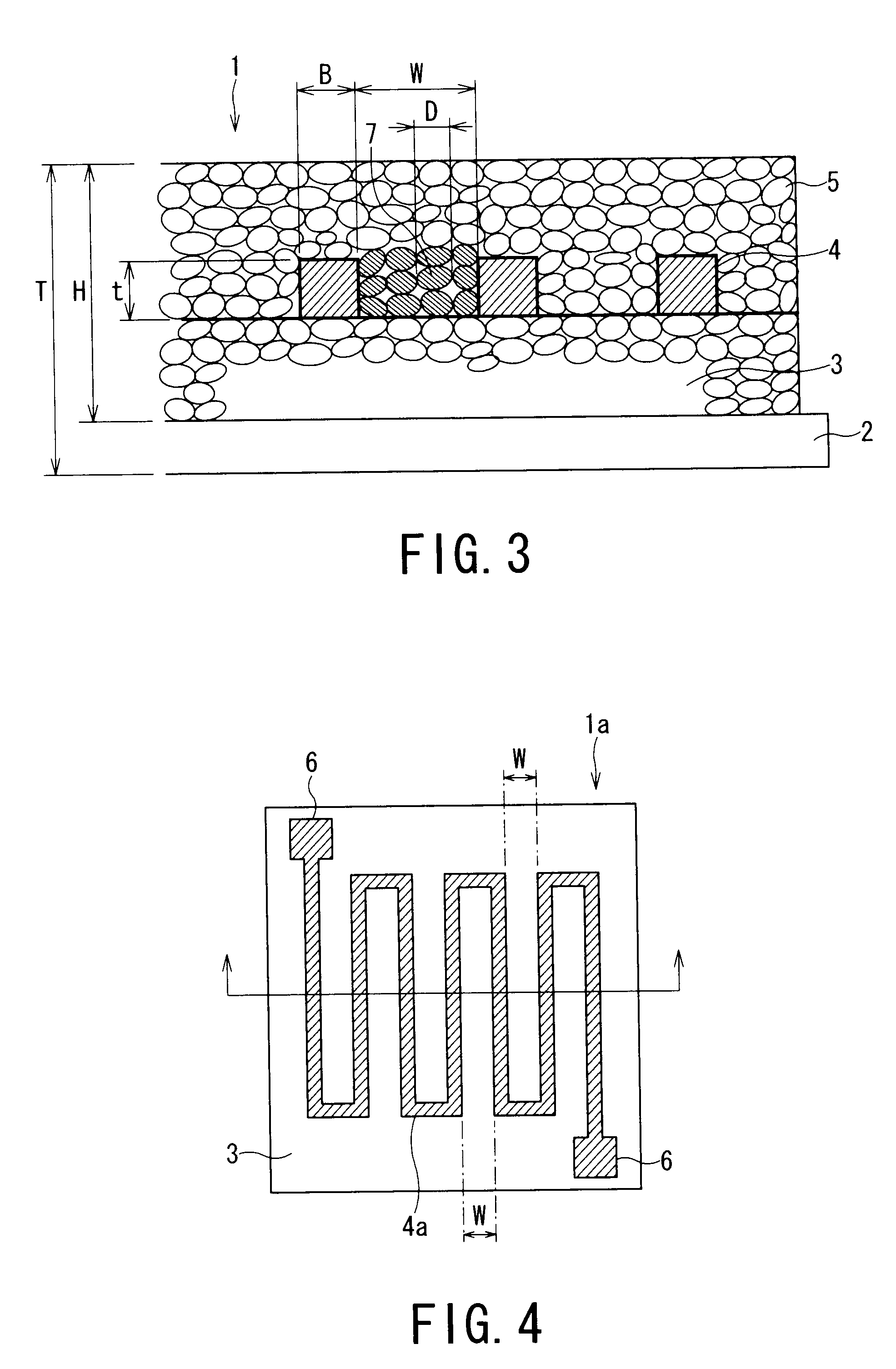
[0068]Each of inductors according to Examples 3 to 11 serving as planar magnetic devices was prepared by forming a first magnetic layer 3 on a Si substrate used in Example 1 by using the above described magnetic paste, followed by forming a planar coil having an inter-coil gap of W shown in Table 1 by using an Ag paste, and forming a second magnetic layer having a predetermined thickness by using the same magnetic paste.

[0069]The magnetic particles used in Examples 3 and 5 has a crude and coarse particle diameter while the magnetic pa...


PUM

PropertyMeasurementUnit
thicknessaaaaaaaaaa
sizeaaaaaaaaaa
heightaaaaaaaaaa

Abstract

A planar magnetic device 1 including a first magnetic layer 3, a second magnetic layer 5, and a planar coil 4 disposed between the first magnetic layer 3 and the second magnetic layer 5, wherein magnetic particles 7 having a shape ratio S/L of 0.7 to 1 when a length of a long axis is L and a length of a short axis orthogonal to the long axis is L are filled in a gap W between coil wirings of the planar coil 4. According to the planar magnetic device 1, it is possible to realize a planar magnetic device such as an inductor reduced in height by using fine particles that enable to effectively obtain a large inductance value.

Description

TECHNICAL FIELD[0001]The present invention relates to a planar magnetic device (magnetic passive device) used as a thin inductor and, particularly, to a planar magnetic device improved in inductance by increasing magnetic permeability to a magnetic field generated in a planar coil as well as to a power source IC package using the same.BACKGROUND ART[0002]In recent years, various electronic appliances have actively been downsized, and there is a tendency of manufacturing various devices by using a thin film process along with such downsizing. Under the circumstances, as a magnetic device such as an inductor (reactor), a trance, and a magnetic head, there has been proposed a planar magnetic device (flat inductor) having a shell type structure wherein a planar coil having a spiral shape or a zigzag pattern (meander type) coated with a magnetic substance in place of a conventional structure having a bulk magnetic material provided with a coil, and attempts have been made for downsizing ...

Claims


Application Information

Patent Timeline
Patent Type & Authority Applications(United States)
IPC IPC(8): H01F5/00
CPCH01F1/15366Y10T428/29H01F1/37H01F17/0006H01F17/04H01F41/046H01F2017/0066H01F2017/0073H01L23/645H01L25/165H01L2224/48247H01L2924/01078H01L2924/01079H01L2924/19041H01L2924/19104H01L2924/30107H01L2924/3011H01L2924/3025H01L24/48H01L2924/01021Y10S428/928H01L2924/07802H01F1/26H01L2924/00H01L2924/181H01L2224/48091H01L2924/14H01L2924/00014H01L2924/00012H01L2224/45099H01L2224/45015H01L2924/207H01F27/255H01F1/20
Inventor INOUE, TETSUOSATO, AKIRANAKAGAWA, KATSUTOSHI
Owner KK TOSHIBA
Why Eureka
Try Eureka