Process of making a microelectronic light-emitting device on semi-conducting nanowire formed on a metallic substrate

a technology of semi-conducting nanowires and light-emitting devices, which is applied in the direction of polycrystalline material growth, crystal growth process, chemically reactive gas growth, etc., can solve the problem of high dislocation rate in the other semi-conducting layers, cumbersome method, and inability to homogeneous current injection on the lower face of the diod

Active Publication Date: 2009-10-01
CENT NAT DE LA RECHERCHE SCI
View PDF8 Cites 15 Cited by
  • Summary
  • Abstract
  • Description
  • Claims
  • Application Information

AI Technical Summary

Problems solved by technology

Lattice mismatch between the sapphire (substrate) and GaN of the buffer layer is generally large, which induces a high rate of dislocations in the other semiconducting layers.
On the other hand, taking into account the insulating character of sapphire, the making of the lower contact requires etching of the active layer 4, which makes the making method cumbersome.
With such an arrangement of the lower contact, current injection is not homogeneous on the lower face of the diode.
When the current passes inside the diode, the result is significant heating of the device by the Joule effect.
This significant heating due to poor dissipation of heat by the substrate 1 (the heat conductivity of the sapphire substrates generally being of the order of 35-40 W / mK), may induce fast degradations of the material and reduce the reliability of the active layer of the LED.
Such a kind of heating may reduce the electric properties of the active layer and deteriorate the yield of the LED.
The electrical performances and those in terms of yield of such a device may prove to be insufficient.

Method used


Image

  • Process of making a microelectronic light-emitting device on semi-conducting nanowire formed on a metallic substrate
  • Process of making a microelectronic light-emitting device on semi-conducting nanowire formed on a metallic substrate
  • Process of making a microelectronic light-emitting device on semi-conducting nanowire formed on a metallic substrate

Examples


Embodiment Construction

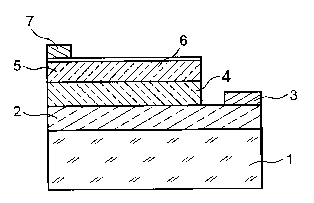
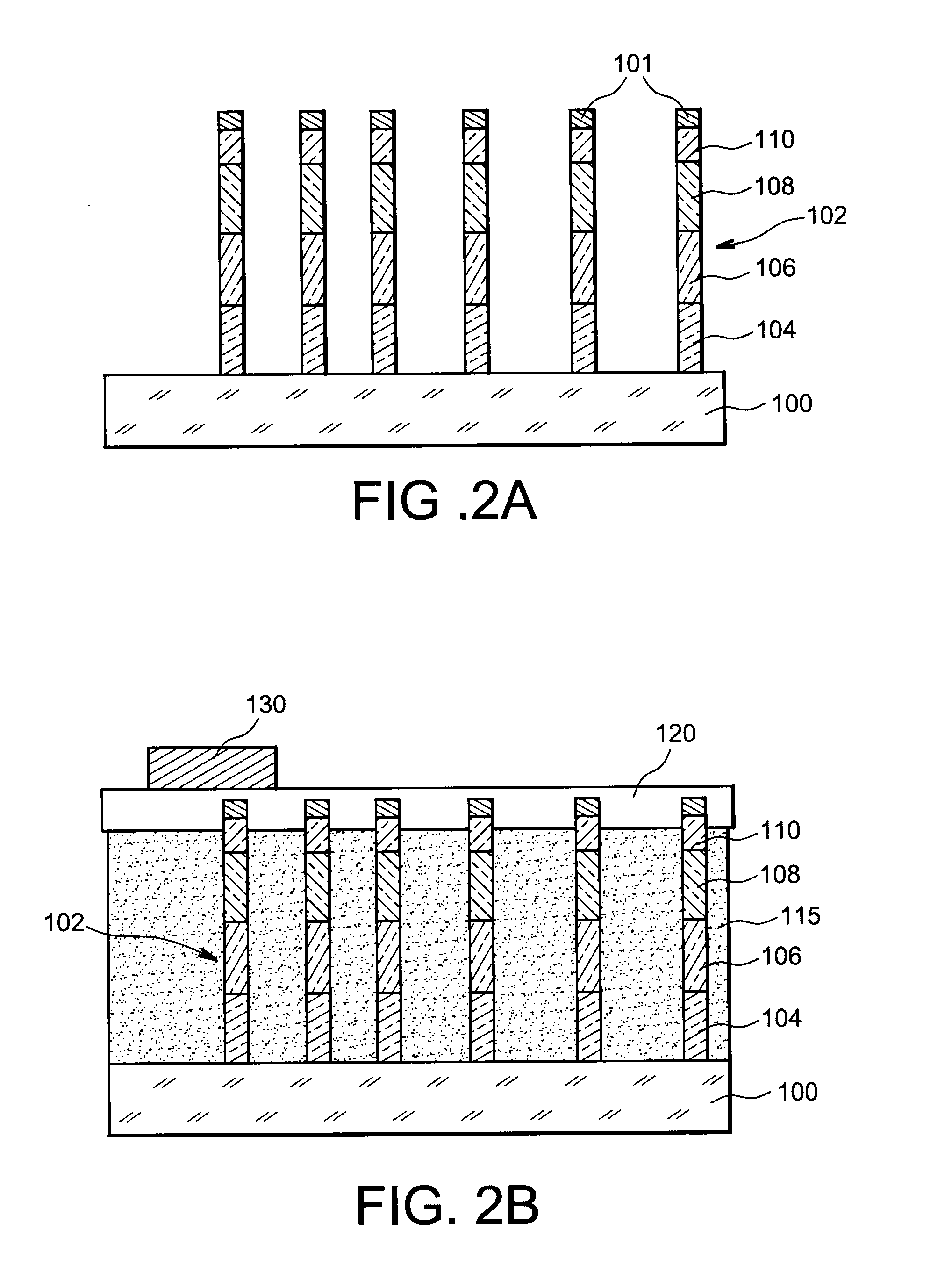
[0028]An exemplary method for making, according to the invention, a light-emitting (LED) microelectronic device, will now be given in connection with FIGS. 2A-2D. The starting material of the method is a substrate 100 which may be based on a metal, for example such as aluminium or silver or copper, or a metal alloy for example based on aluminium or silver or copper, or such as stainless steel or a FeNi alloy, including iron and nickel such as Invar® (registered trade mark by Goodfellow). The metal substrate 100 may have a thickness for example comprised between 10 μm and 10 mm, or for example of the order of 1 mm, and a surface for example comprised between 100 mm2 and 1 m2, or for example of the order of 300 mm2.

[0029]A step for preparing the substrate 100 and in particular a given face of the latter with view to growing wires based on one or several semiconducting materials, may be achieved by means of a surface treatment, for example comprising a step for degreasing the substrate...


PUM

PropertyMeasurementUnit
sizeaaaaaaaaaa
thicknessaaaaaaaaaa
thicknessaaaaaaaaaa

Abstract

A process of making a microelectronic light-emitting device, including: a) growth on a metallic support of multiple wires based on one or more semi-conducting materials designed to emit radiant light, and b) formation of at least one electrical conducting zone of contact on at least one of the wires.

Description

TECHNICAL FIELD[0001]The technical field to which relates the invention is that of microelectronics and optoelectronics and more specifically the making of light emitters based on semiconducting materials.[0002]The invention relates to a method for making a light-emitting device comprising a plurality of nanowires formed on a metal substrate.PRIOR ART[0003]The making of a light-emitting microelectronic device, for example of the LED (<<Light Emitting Device>> or electroluminescent device) type may be currently carried out with successive epitaxies of several thin layers of semiconducting materials. Sapphire-based substrates, or substrates based on silicon carbide are generally used for forming this type of device. The size of these substrates is often smaller than 3 inches (7.62 centimeters), which limits the number of LEDs which may be integrated onto a same substrate.[0004]For example, for a LED emitting light at 450 nm, the following stack may be made: on a sapphire t...

Claims


Application Information

Patent Timeline
Patent Type & Authority Applications(United States)
IPC IPC(8): H01L21/3205H01L33/08H01L33/20H01L33/24H01L33/32
CPCC30B25/00C30B29/403C30B29/605H01L33/08H01L33/20H01L2924/0002H01L33/24H01L33/32H01L2924/00H01L33/007H01L33/06H01L33/18H01L33/38H01L33/50
Inventor GILET, PHILIPPEFERRET, PIERREGENTILE, PASCALTCHELNOKOV, ALEXEIBARON, THIERRY
Owner CENT NAT DE LA RECHERCHE SCI
Why Eureka
Try Eureka