Semiconductor device and method for manufacturing the same

a technology of metallic oxide film and semiconductor, which is applied in the direction of semiconductor devices, transistors, electrical devices, etc., can solve the problems of reduced yield, difficult process correction, and inability to control the threshold voltage (vth) of tft in the subsequent process, so as to reduce the distribution of oxide fet, improve the characteristics of oxide fet, and reduce yield

Inactive Publication Date: 2009-10-22
HITACHI LTD
View PDF4 Cites 206 Cited by
  • Summary
  • Abstract
  • Description
  • Claims
  • Application Information

AI Technical Summary

Benefits of technology

[0031]According to the semiconductor device and the manufacturing method thereof, the improvement in characteristics of the oxide FET and the decrease of the distribution thereof can be made by decreasing the contact resistance, the parasitic resistance, and the variations thereof.
[0032]Moreover, by controlling Vth after forming the source region and the drain region or the source electrode and the drain electrode, the reduction in yield in the ca

Problems solved by technology

However, in a method disclosed in JP-A-2007-073699, since the carrier concentration in the channel region is determined while depositing the metallic oxide film, there is a problem that the threshold voltage (Vth) of the TFT cannot be controlled in the subsequent processes, for instance, after the source region and drain region or source electrode and drain electrode are formed.
Therefore, there is a problem that a reduction in yield easily occurs in the case of mass-production of a TFT and, for instance, that process corrections are difficult when there is a change in the product type to which the TFT is applied.
Moreover, there is another problem that it is impossible to manufacture TFTs having different threshold voltages (Vth) over the same substrate and the degree of freedom of the circuit design is low.
In addition, although the bottom-gate type TFT is generally easy to manufacture and suitable for mass-production, there is a problem that it is impossible to manufacture the bottom-gate type TFT by using the disclosed method.
However, even in a method disclo

Method used


Image

  • Semiconductor device and method for manufacturing the same
  • Semiconductor device and method for manufacturing the same
  • Semiconductor device and method for manufacturing the same

Examples


first embodiment

(Configuration and Manufacturing Method)

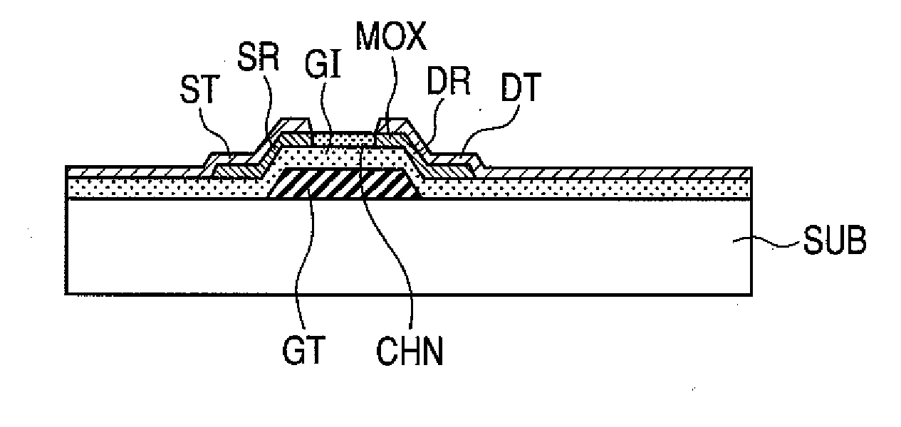
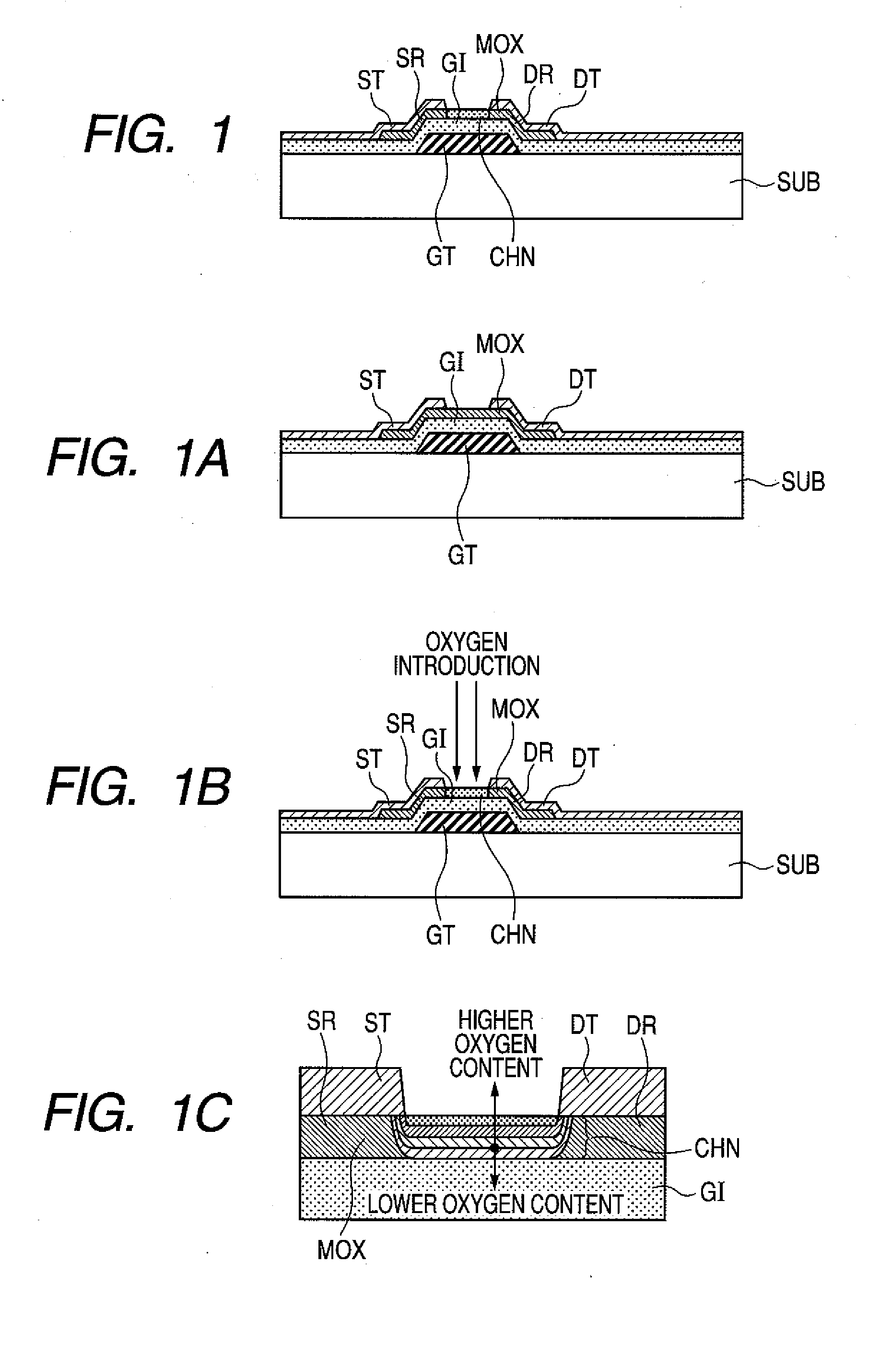
[0050]FIG. 1 is a configuration illustrating the first embodiment of a semiconductor device according to the present invention. A so-called bottom-gate type oxide TFT is shown as a semiconductor device. As shown in FIG. 1, a gate electrode GT is formed over a substrate SUB. Then, a gate insulator film GI is formed over the top surface of the substrate SUB covering the aforementioned gate electrode GT. In addition, a metallic oxide film MOX is formed over the aforementioned gate insulator film GI extending over at least the aforementioned gate electrode GT. Moreover, a source electrode ST and a drain electrode DT are formed directly in contact with the aforementioned metallic oxide film MOX. The source electrode ST and the drain electrode DT are separated on at least the gate electrode GT and formed opposing each other and existing between this separation part. Herein, the aforementioned metallic oxide film MOX consists of a channel region CHN ...

second embodiment

(Configuration and Manufacturing Process)

[0062]FIG. 5 is cross-sectional drawings illustrating the second embodiment of the semiconductor device in the present invention. FIG. 5 is drawings where two kinds of bottom-gate type oxide TFTs with different Vth are formed over the same substrate.

[0063]That is, the oxide TFT 1 and the oxide TFT 2 are formed over the top surface of the substrate SUB 1. These oxide TFT 1 and oxide TFT 2 have almost the same stacking structure of the material layers constituting them; the Vth is made higher in the oxide TFT 1; and the Vth is made lower in the oxide TFT 2. That is, the oxygen content introduced into the oxide TFT 1 is made higher than that in the source region SR and the drain region DR in the channel region CHN, and the oxide TFT 2 is formed to have no oxygen content difference from the source region SR and the drain region DR in the channel region CHN.

[0064]FIGS. 5A and 5B are explanatory drawings illustrating a manufacturing method of a sem...

third embodiment

(Configuration and Manufacturing Process)

[0067]FIG. 6 is cross-sectional drawings illustrating the third embodiment of the semiconductor device in the present invention and they are drawings corresponding to FIG. 5. As well as the case of FIG. 5, FIG. 6 is drawings where two kinds of bottom-gate type oxide TFTs with different Vth are formed over the same substrate. The configuration which is different from the case of FIG. 5 is that oxygen is introduced into the channel region CHN in the oxide TFT 2 and the content thereof is made lower than the oxygen content of the channel region CHN in the oxide TFT 1.

[0068]FIGS. 6A and 6B are explanatory drawings illustrating a manufacturing method of a semiconductor device shown in FIG. 6. First of all, the oxide TFT 1 and the oxide TFT 2 are formed to be the structure shown in FIG. 1B by using a general manufacturing process and the manufacturing process disclosed in this specification (FIG. 6A). At this stage, the same amount of oxygen is int...


PUM


Abstract

A metallic oxide semiconductor device with high performance and small variations. It is a field effect transistor using a metallic oxide film for the channel, which includes a channel region and a source region and comprises a drain region with a lower oxygen content than the channel region in the metallic oxide, in which the channel region exhibits semiconductor characteristics and the oxygen content decreases with depth below the surface.

Description

CLAIM OF PRIORITY[0001]The present application claims priority from Japanese patent application JP 2008-106586 filed on Apr. 16, 2008, the content of which is hereby incorporated by reference into this application.FIELD OF THE INVENTION[0002]The present invention relates to a semiconductor device and a method for manufacturing the same and more particularly to a field-effect transistor using a metallic oxide film for a channel and a manufacturing method thereof.BACKGROUND OF THE INVENTION[0003]Recently, attempts have been made to form a field-effect transistor (hereinafter, it may be called simply FET in this specification) using a metallic oxide film for a channel layer. Especially, thin film transistors, using ZnO, InGaZnO, and ZnSnO, etc. for a channel layer (hereinafter, it may be called simply TFT in this specification) have been developed. However, the main motive thereof is that the manufacturing process being performed at low temperatures and being simple. Research and devel...

Claims


Application Information

Patent Timeline
IPC IPC(8): H01L29/786H01L21/336
CPCH01L27/1214H01L29/7869H01L27/1225H01L27/127
Inventor KAWAMURA, TETSUFUMISATO, TAKESHIHATANO, MUTSUKOUCHIYAMA, HIROYUKI
Owner HITACHI LTD
Why Eureka
Try Eureka