Method of mounting electronic circuit constituting member and relevant mounting apparatus

a technology of electronic circuit and mounting apparatus, which is applied in the direction of printed circuit manufacturing, coating, conductive pattern formation, etc., can solve the problems of high manufacturing cost, high manufacturing cost, and the inability to form crystalline semiconductor transistors on glass substrates, etc., and achieves accurate mounting and good reproducibility

Inactive Publication Date: 2009-10-29
PANASONIC CORP
View PDF13 Cites 58 Cited by
  • Summary
  • Abstract
  • Description
  • Claims
  • Application Information

AI Technical Summary

Benefits of technology

[0011]Under these circumstances, an object of the present invention is to provide a novel method and apparatus for accurately mounting electronic circuit-constituting members on a predetermined position of a substrate with good reproducibility, when these members, such as component chips and nanomembers are mounted on the substrate.

Problems solved by technology

With current technology, however, crystalline semiconductor transistors cannot be formed on the glass substrate, and for this reason thin film transistors formed of an amorphous silicon or polysilicon thin film have been used for the control of the pixels.
Providing the openings in the glass substrate requires expensive equipment such as a laser processing device.
Therefore, one of the big challenges, in order to fabricate the field-effect transistors of a coating type using nanomembers, is the precise control of the orientation and position of the nanomembers in mounting the nanomembers on the substrate.
This has posed the problem of high manufacturing cost.
However, it has difficulties in controlling the amount of liquid disposed on the mating surfaces (Sensor Update, Vol. 13, P 3, 2004).
Specifically, when the amount of liquid is too small, the contact surface between the substrate and the member will not be completely covered with the liquid and the adhesion is weak.
On the other hand, when the amount of liquid is too large, the members will float on the liquid surface and move around, causing a problem that the members will detach from the liquid even with little stirring.
Another drawback of this method is the low dispersibility of the members to the dispersion medium due to the two kinds of member surfaces with dissimilar properties (water-repellent mating surface and the hydrophilic surface in the remaining portion).
This causes a problem that the members will adhere to the air / liquid interface of the dispersion medium, or agglomerate.
Further, with nano-scale members, it is technically difficult to provide different wettability to different portions of the surface.
This has made the placement of the nano-scale members on a substrate difficult.
When the conventional flow method is used to control the orientation and position of the pillar-like nanomembers in mounting these members on a substrate, there are difficulties in stably orienting and positioning the members.
Further, since this method uses a mold that regulates the direction of a liquid flow, it requires complicated fabrication steps and therefore complex equipment.
Because of this, the method has the problem of high manufacturing cost and poor reproducibility.
Further, accurate orientation of the nanomembers is difficult to achieve with the conventional method utilizing the liquid / solid / gas interface.
The method therefore requires complex equipment, which poses the problem of high manufacturing cost and poor reproducibility.

Method used


Image

  • Method of mounting electronic circuit constituting member and relevant mounting apparatus
  • Method of mounting electronic circuit constituting member and relevant mounting apparatus
  • Method of mounting electronic circuit constituting member and relevant mounting apparatus

Examples


first embodiment

[0121]In the First Embodiment, a mounting method of the present invention will be described in detail with reference to the drawings. In the present embodiment, the description will be directed to the case where the electronic circuit-constituting member is a component chip including an electronic device, and the component chip is mounted on a substrate.

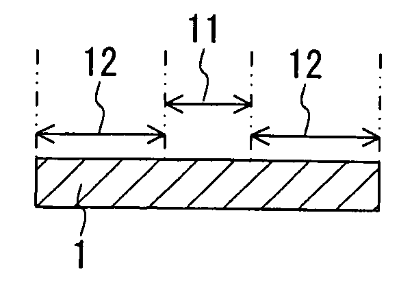
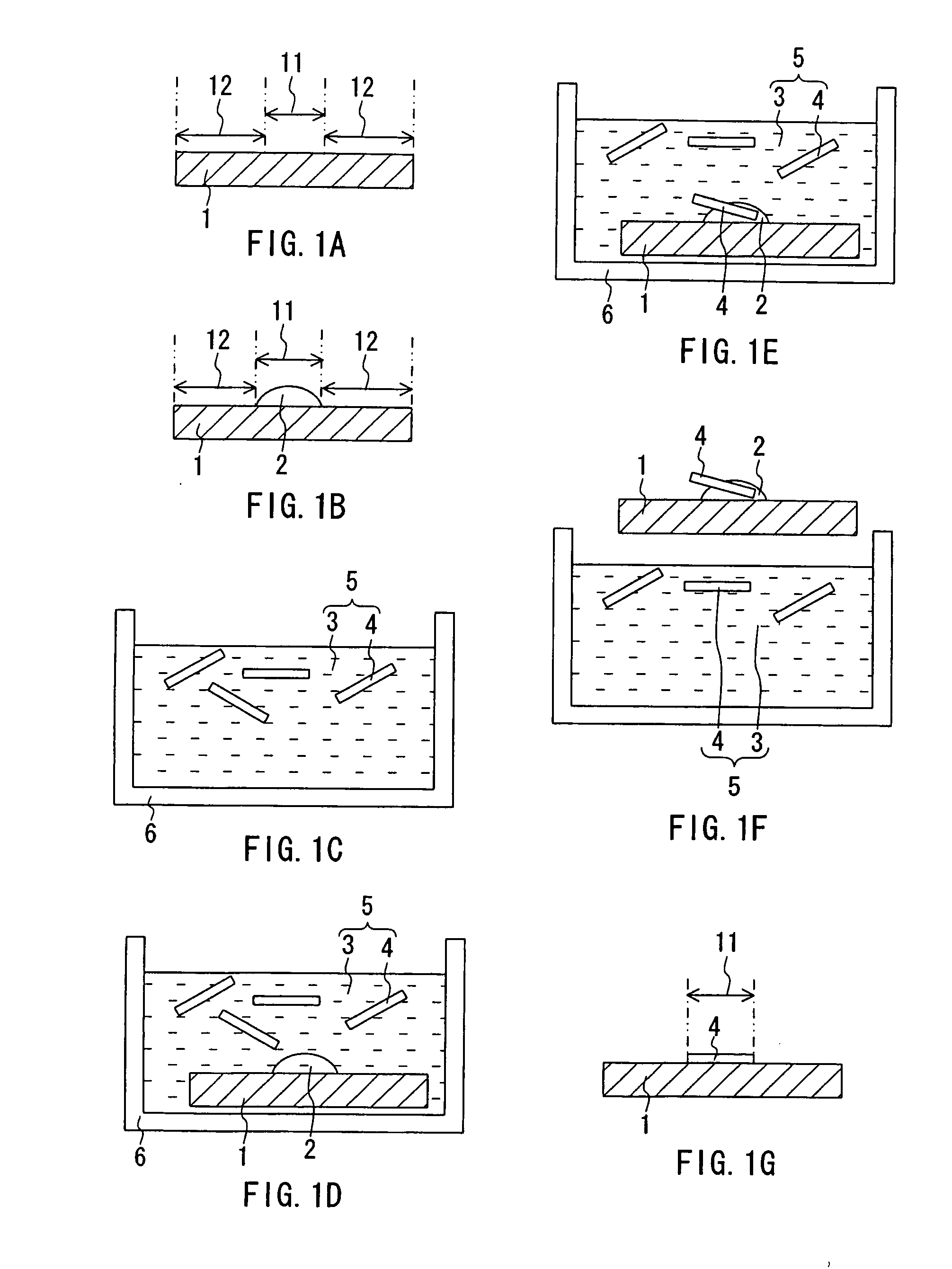
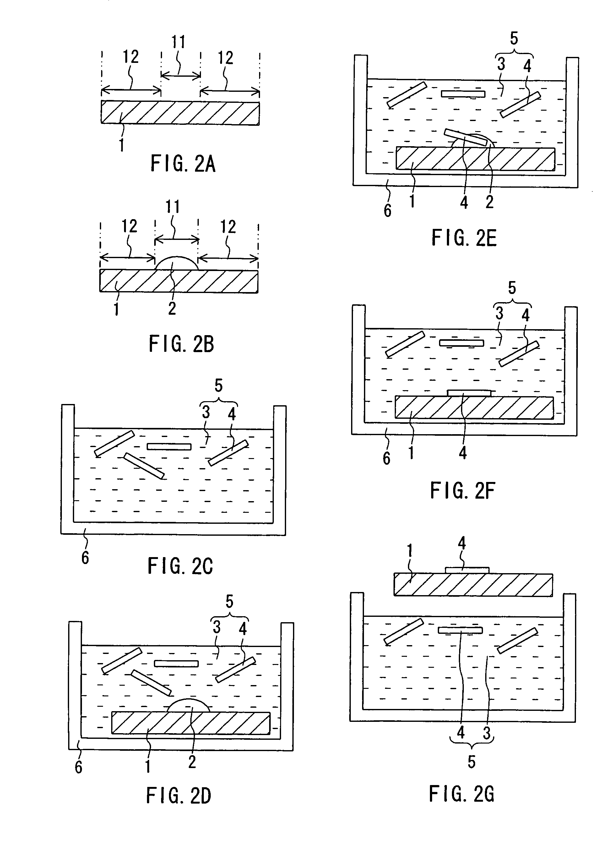
[0122]FIG. 1A to FIG. 1G, and FIG. 3A and FIG. 3B schematically illustrate respective steps of a mounting method of the present embodiment. First, a substrate 1 as shown in FIG. 1A and FIG. 3A is prepared. On one principal surface of the substrate 1 are provided a first region 11 and a second region 12 surrounding the first region 11. The first region 11 and the second region 12 are formed such that the first region 11 is more wettable than the second region 12 with respect to the first liquid described later. As shown in FIG. 3A, the first region 11 is rectangular in shape. In the following, the surface of the substrate 1 provided w...

second embodiment

[0168]In the Second Embodiment below, the description is directed to a fabrication method of an electronic instrument of the present invention, and a display device fabricated by the fabrication method, with reference to the drawings. The following description of the present embodiment will be given based on a fabrication method of a display device, or more specifically a liquid crystal display, as an example of the electronic instrument. It should be noted that the present invention is not limited by the following description.

[0169]FIG. 14 schematically illustrates a partial configuration of a liquid crystal display 140 as an electronic instrument of the present embodiment.

[0170]The liquid crystal display 140 includes a glass substrate 141, an X driver 142, a Y driver 143, X scanning electrodes 144, Y scanning electrodes 145, transistor chips (component chips) 146, and pixel portions 147. The transistor chips 146 are monocrystalline silicon transistors.

[0171]The pixel portions 147 ...

third embodiment

[0191]In the Third Embodiment below, the description is directed to a fabrication method of an electronic instrument of the present invention, and a display device fabricated by the fabrication method, with reference to the drawings. The description of the present embodiment will be given based on a fabrication method of a display device, or more specifically an organic electroluminescence display (organic EL display) as an example of an electronic instrument. The present invention is not limited by the following description.

[0192]FIG. 17 schematically illustrates a configuration of an organic EL display 200 of the present embodiment.

[0193]The organic EL display 200 includes a substrate 201 made of polycarbonate, an X driver 202, a Y driver 203, X scanning electrodes 204, Y scanning electrodes 205, component chips 206 and pixel portions 207. The component chips 206 each include a crystalline silicon transistor circuit. The pixel portions 207 include organic EL material, and are cont...


PUM

PropertyMeasurementUnit
lengthaaaaaaaaaa
sizeaaaaaaaaaa
diameteraaaaaaaaaa

Abstract

A mounting method comprising the steps of (A) disposing first liquid (2) on first region (11) provided on one principal surface of substrate (1); (B) bringing member-containing liquid (5) containing second liquid (3) and at least one member (4) into contact with the first liquid (2) disposed on the first region (11); and (C) removing the first liquid (2) and the second liquid (3) from the one principal surface to thereby dispose the member (4) on the first region (11). The first liquid (2) is substantially not dissolved in the second liquid (3). The wettability of the first liquid (2) with respect to the surface of the member (4) is higher than that of the second liquid (3).

Description

TECHNICAL FIELD[0001]The present invention relates to a method and apparatus for mounting electronic circuit-constituting members.BACKGROUND ART[0002]Active-matrix liquid crystal display elements and organic electroluminescence display elements are formed on a glass substrate. The pixels disposed in a matrix on the substrate are controlled by the transistors provided in the vicinity of the pixels. With current technology, however, crystalline semiconductor transistors cannot be formed on the glass substrate, and for this reason thin film transistors formed of an amorphous silicon or polysilicon thin film have been used for the control of the pixels. The thin film transistor has the advantage that it can be formed on a large-area substrate at low cost; however, its smaller mobility compared with crystalline silicon has prevented them from operating at high speed. To overcome such a problem, there have been proposed techniques in which the transistors first are fabricated on a silicon...

Claims


Application Information

Patent Timeline
Patent Type & Authority Applications(United States)
IPC IPC(8): H05K3/10C23C16/00
CPCH01L21/67144Y10T29/49155H01L24/83H01L24/95H01L25/0655H01L2224/83136H01L2224/83192H01L2224/8385H01L2224/95085H01L2224/95102H01L2224/95146H01L2924/01005H01L2924/0101H01L2924/01013H01L2924/01015H01L2924/01027H01L2924/01029H01L2924/01032H01L2924/01033H01L2924/01047H01L2924/01052H01L2924/01078H01L2924/01079H01L2924/07802H01L2924/09701H01L2924/14H01L2924/19041H01L2924/19042H01L2924/19043H01L2924/30107H01L2224/2919H01L2924/01006H01L2924/01019H01L2924/01023H01L2924/0665H01L24/75Y10T29/49133Y10T156/10Y10T29/4913Y10T29/49128H01L2924/1306H01L2924/10253H01L2924/00H01L2924/15788
Inventor NAKAGAWA, TOHRUTORII, HIDEO
Owner PANASONIC CORP
Why Eureka
Try Eureka