

Film-forming apparatus, film-forming method and recording medium
- Summary
- Abstract
- Description
- Claims
- Application Information
AI Technical Summary
Benefits of technology
Problems solved by technology
Method used
Image

Examples
embodiment 1
[0127]FIG. 12 is a diagram schematically showing a film forming apparatus 30 in an embodiment 1 of the present invention.
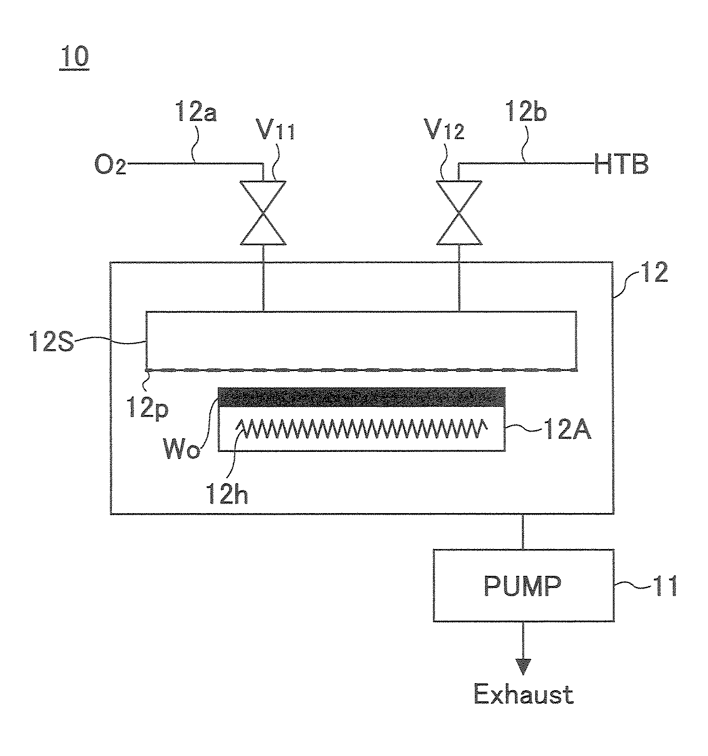
[0128]As shown in FIG. 12, the film forming apparatus 30 has a processing chamber 32 that is exhausted by a pump 31. A to-be-processed substrate W made of silicon, for example, is held within the processing chamber 32 by a holding base 32A that has a heating means 32h embedded therein.
[0129]A shower head 32S is also provided within the processing chamber 32 so as to confront the to-be-processed substrate W. A line 32a for supplying oxygen gas is connected to the shower head 32S via an MFC (Mass Flow Controller) which is not shown and a valve V31.
[0130]The film forming apparatus 30 of this embodiment further has a first gas supplying means G1, within the processing chamber 32, for supplying a first vapor source including a metal alkoxide (for example, HTB) having a tertiary butoxyl group as a ligand, and a second gas supplying means G2, within the processing chambe...
embodiment 2
[0157]In the film forming apparatus 30 described above, the pre-reaction means is not limited to the structure of the embodiment 1 described above, and various variations and modifications may be made, as described below.
[0158]For example, FIG. 18 is a diagram schematically showing a cross section of a pre-reaction means 150 in the embodiment 2 of the present invention. In FIG. 18, those parts that are the same as those of the preceding figures are designated by the same reference numerals, and a description thereof will be omitted.
[0159]As shown in FIG. 18, the pre-reaction means 150 of this embodiment has a spiral pipe 150a in which the first vapor source and the second vapor source are mixed. The gas lines 32b and 32c are connected to one end of the pipe 150a, and the supply line 103 is connected to the other end of the pipe 150a. Since the pipe 150a has the spiral shape, it is possible to form a long pipe compared to a straight pipe within a given space. Because the pipe 150a ca...
embodiment 3
[0160]When causing the pre-reaction by the pre-reaction means, a film formation on the inner walls of the reaction chamber, for example, may become a problem depending on the conditions of the pre-reaction. Hence, in order to suppress the amount of film formation on the inner walls of the reaction chamber, the pre-reaction means may be configured as follows, for example.
[0161]FIG. 19 is a diagram schematically showing a cross section of a pre-reaction means 200 in the embodiment 3 of the present invention. In FIG. 19, those parts that are the same as those of the preceding figures are designated by the same reference numerals, and a description thereof will be omitted.
[0162]As shown in FIG. 19, a pre-reaction means 200 of this embodiment has the reaction chamber 100a and a multi-hole cylinder 201 that is inserted inside the reaction chamber 100a. The multi-hole cylinder 201 has an approximate cylindrical shape and a large number of gas ejection holes 201a formed in the wall thereof....
PUM
| Property | Measurement | Unit |
|---|---|---|
| Temperature | aaaaa | aaaaa |
| Temperature | aaaaa | aaaaa |
| Temperature | aaaaa | aaaaa |
Abstract
Description
Claims
Application Information