

Circuits, processes, devices and systems for full integration of RF front end module including RF power amplifier
a power amplifier and front end module technology, applied in the field of wireless communication and electronics, can solve the problems of partial integration not attractive, no t/r switch integration or t/r switch elimination has been achieved so far, and achieve the effect of increasing the signal-to-noise ratio
- Summary
- Abstract
- Description
- Claims
- Application Information
AI Technical Summary
Benefits of technology
Problems solved by technology
Method used
Image

Examples
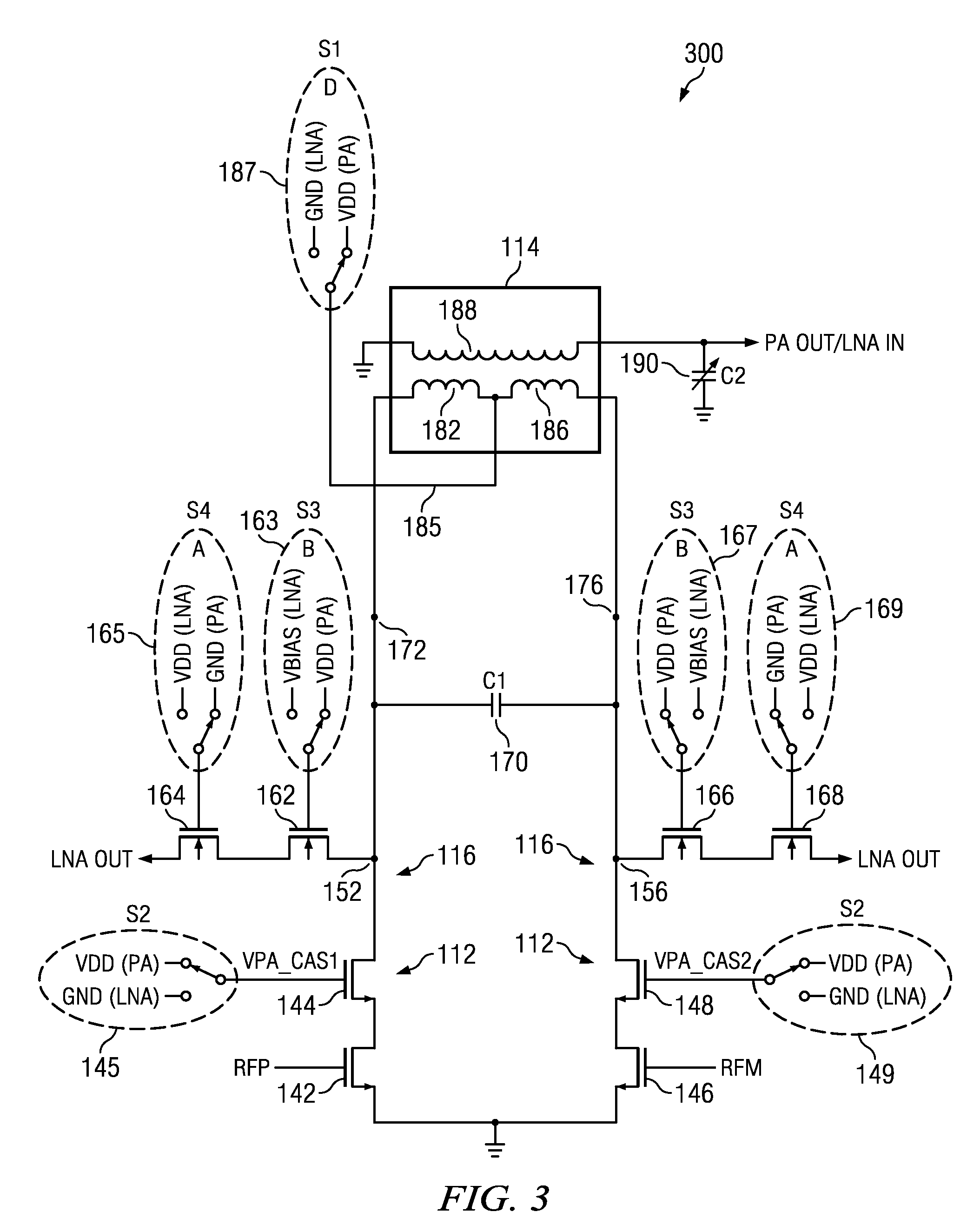
embodiment 300
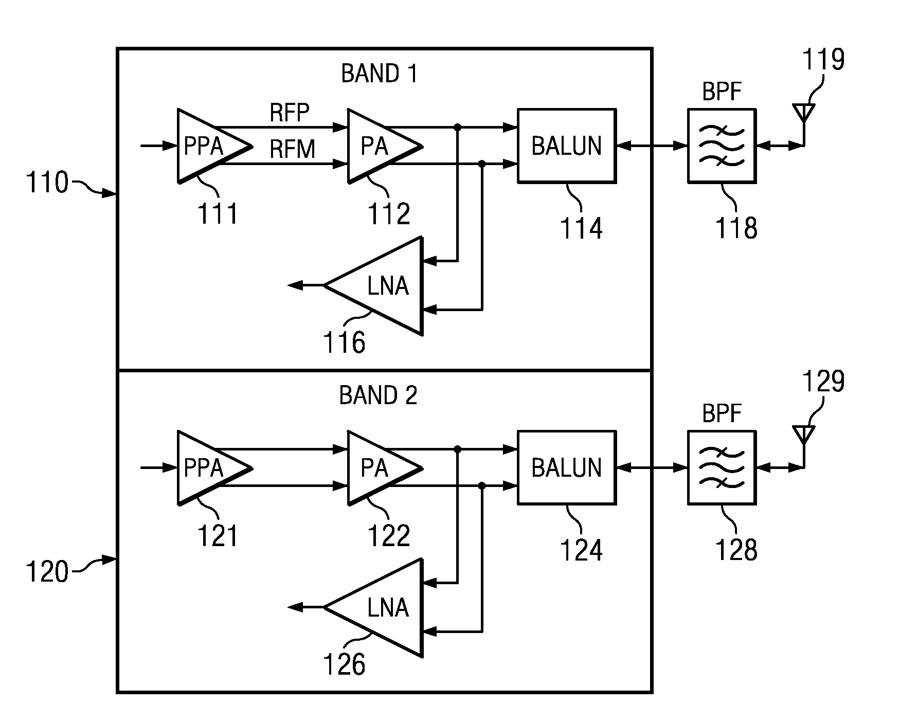
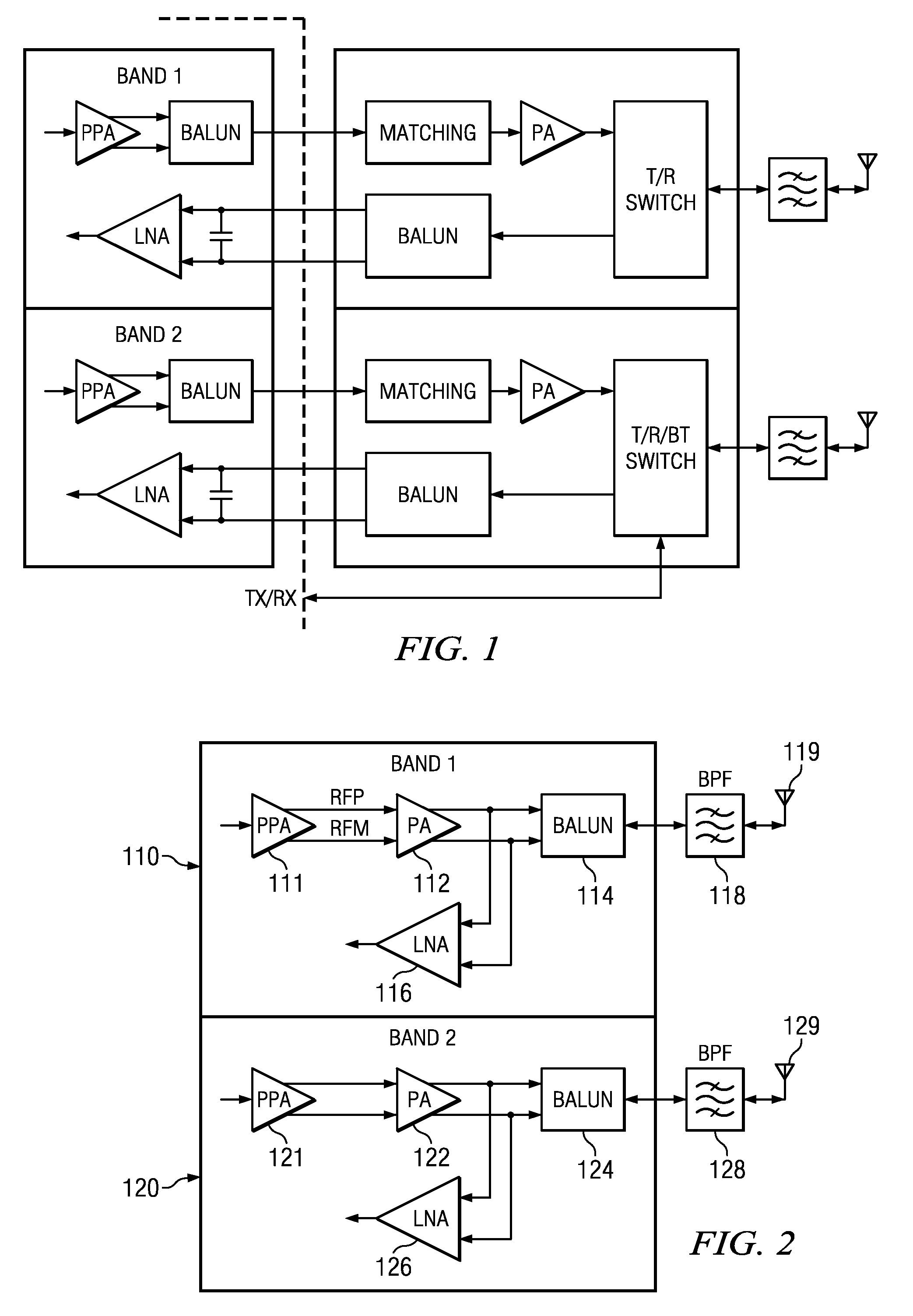
[0035]In FIG. 3, a PA-plus-LNA circuit embodiment 300 has T / R Switch Elimination Power switches in non-signal path are used instead of transmit / receive (T / R) switching. Insertion loss of signal due to T / R switch is eliminated by direct ohmic connection along with N:1 balun transformer for better LNA noise match and PA power optimization. As an extension, the balun transformer can be replaced with a matching network or additional matching network can be used at the primary or secondary side.
[0036]In FIG. 3, DC power current runs via the center tap 185 through the balun itself to the PA 112 and PA 112 conversely delivers amplified RF to balun 114, instead of embodiment 300 capacitively coupling only RF between PA 112 and balun 114. An integrated balun (on-chip) 114 integrated in a CMOS process has acceptable insertion loss comparable to the insertion loss of external (off-chip) low-cost baluns and handles the DC and RF currents involved in power amplifier PA 112 operation. Thus an ext...
embodiment 500
[0061]In FIG. 5, a PA-plus-LNA circuit embodiment 500 provides LNA gain switching and programmability for WLAN and / or other telecommunications applications. Two LNA tap sections are provided. The first LNA tap section is exteriorly connected to balun 114 via lines 172 and 176 as in FIG. 3 and has LNA transistors 162, 164, 166, 168 with supporting switches 163, 165, 167, 169. The second LNA tap section is interiorly connected to balun 114 via lines 452 and 456 in FIG. 5 and has analogously-numbered LNA transistors 462, 464, 466, 468 with supporting switches 463, 465, 467, 469. In FIG. 5, all components having same numerals as in FIG. 3 operate the same way as in FIG. 3, and all added tap section components in FIG. 5 having analogous 4xx numerals operate in an analogous manner to those components with corresponding 1xx numerals in FIG. 3.
[0062]In the FIG. 5 gain programming, the control switching of FIGS. 4A / 4B enables one at a time of the LNA tap sections so that the LNA transistors ...
embodiment 600
[0067]In FIG. 6, the same transistors 142, 146 and 144, 148 operate in different balanced operating modes as either a PA or LNA in an alternative circuit embodiment 600. FIG. 6 shows the PA-plus-LNA circuit 600 with same transistors used for LNA and PA for WLAN, cellular or other telecommunications. Also in FIG. 6, the same transistor 144 (148) is used as both a power amplifier output transistor (as in FIG. 3) and re-used as an LNA input transistor (analogous to FIG. 3 transistor 162 (166)). This approach of double use or reuse reduces extra routing and real estate in the chip layout and reduces associated signal and power loss. Thus the FIG. 6 transistors 144, 148 act as balanced current buffer PA 112 output devices or as transconductors (voltage to current converter) as if in the FIG. 3 LNA 116 balanced RF amplifier. Further in FIG. 6, the same transistor 142, 146 is used as both a PA 112 input amplifier transistor (as in FIG. 3) and re-used as an LNA output buffer transistor (ana...
PUM
 Abstract
Description
Claims
Application Information