Ceramic electronic component and method for manufacturing the same

a ceramic electronic component and ceramic technology, applied in the direction of fixed capacitor details, variable capacitors, fixed capacitors, etc., can solve the problems of reliability, prone to blistering at the surface of the plating layer, and the electroless plating layer formed by electroless plating does not have sufficient adhesion to the side surfaces, etc., to achieve high effective volume and high reliability

Active Publication Date: 2009-12-10
MURATA MFG CO LTD
View PDF18 Cites 14 Cited by
  • Summary
  • Abstract
  • Description
  • Claims
  • Application Information

AI Technical Summary

Benefits of technology

[0013]Accordingly, preferred embodiments of the present invention provide a highly reliable ceramic electronic component having high effective volume and a method for manufacturing the same.
[0021]Since the external electrode is substantially composed of at least one plating layer, the ceramic electronic component can exhibit a high effective volume. The plating layer containing metal-coated glass particles can exhibit high adhesion and results in reduced blisters, thus achieving a reliable ceramic electronic component.
[0022]If the plating layer is formed on a surface of the multilayer composite at which internal electrodes are exposed, the glass component of the glass particles fills the interfaces between the ceramic layers and the internal electrode layers by heat treatment, and, thus, prevents liquid or moisture from permeating the multilayer composite through the interfaces. Thus, the resulting monolithic ceramic electronic component is highly reliable.
[0023]In the method for manufacturing the ceramic electronic component according to a preferred embodiment of the present invention, glass particles dispersed in the plating bath are coated with metal films. Consequently, the glass particles can be easily co-deposited with the plating metal. This helps the control of the content and the degree of dispersion of the glass particles in the plating layer. The metal film coating the glass particles hinders the glass particles from being melted in the plating bath and, thus, facilitates the control of the plating bath. In addition, the metal film of the glass particles prevents plating solution from being trapped in asperities of the glass particles and, thus, reduces the occurrence of blisters by heat treatment.
[0024]Furthermore, in the method for manufacturing the ceramic electronic component, the heat treatment performed at a temperature equal to or greater than the softening point of the glass particles after forming the plating layer further enhances the adhesion between the glass component and the ceramic body. Thus, a highly reliable ceramic electronic component can be achieved.

Problems solved by technology

However, the electroconductive metal layer formed by electroless plating does not have sufficient adhesion to the side surfaces.
This may cause a problem with reliability.
In the production process of this external electrode, however, a blister is liable to be formed at the surface of the plating layer by heat treatment performed after electroless plating, depending on the conditions of the heat treatment.
The blister can cause moisture permeation to degrade the reliability, and besides degrades the appearance.
In addition, if the glass particles and the plating metal are co-deposited in this process, the glass is not sufficiently deposited undesirably.
Also, the glass can undesirably be melted and lost in a plating bath.

Method used


Image

  • Ceramic electronic component and method for manufacturing the same
  • Ceramic electronic component and method for manufacturing the same
  • Ceramic electronic component and method for manufacturing the same

Examples


example 1

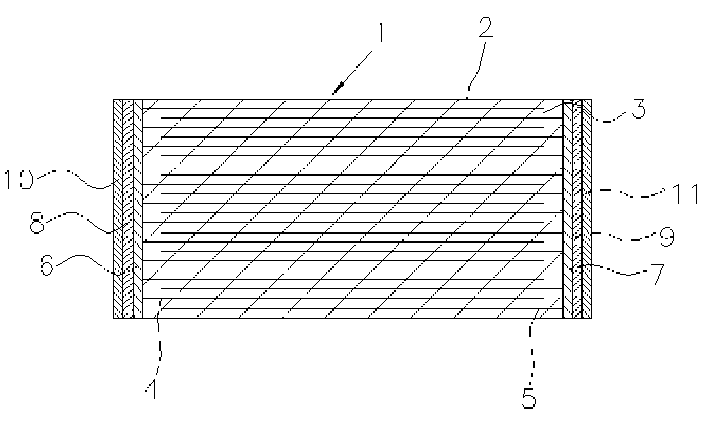
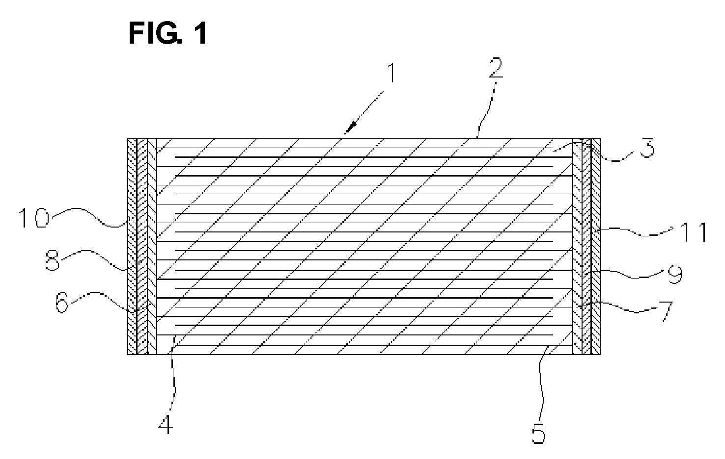
[0056]A multilayer composite of 1.0 mm in length by 0.5 mm in width by 0.5 mm in thickness was prepared for a monolithic ceramic capacitor, and on which plating layers were formed. The dielectric ceramic layers were made of a barium titanate-based dielectric material, and the internal electrodes were essentially made of Ni. Each dielectric ceramic layer between two adjacent internal electrodes had a thickness of about 2 μm, and each internal electrode layer had a thickness of about 1 μm.

[0057]After being dried, the multilayer composite was subjected to sandblasting with an abrasive so that the height of the protrusions of the internal electrodes from the internal electrode-exposing surfaces was about 1 μm on average.

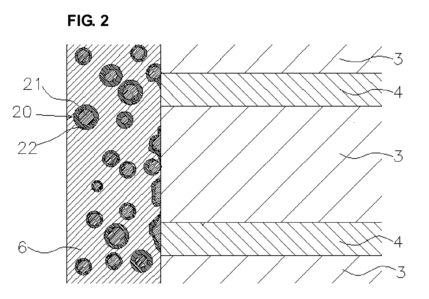
[0058]Then, a B—Si glass powder having a softening point of about 600° C. and an average particle size of 1.1 μm was prepared. The glass powder was subjected to sputtering to give electroconductivity to the surfaces of the powder particles. The powder particles were subs...

example 2

[0068]The same multilayer composite and the same glass particles as in Example 1 were prepared. The glass particles were coated with Ni films in the same manner as in Example 1.

[0069]The Ni-coated glass particles were added to an electroless Cu plating bath containing OPC Copper T produced by Okuno Chemical Industries to a concentration of 30 g / L, and were dispersed by stirring at a bath temperature of 40° C. and a pH of 12.

[0070]Then, 30 mL of multilayer composites and 70 mL of Cu-coated solder balls having a diameter of 0.7 mm were placed in a 300 mL rotation barrel.

[0071]The rotation barrel was immersed in the plating bath and rotated at 12 rpm. As a result, Cu plating layers containing the glass particles were formed to a thickness of 5 μnm on the internal electrode-exposing surfaces of the multilayer composites.

[0072]After being taken out from the rotation barrel, the multilayer composites were heated to a temperature of 700° C. at a rate of 5° C. / min in a nitrogen atmosphere a...


PUM

PropertyMeasurementUnit
thicknessaaaaaaaaaa
particle sizeaaaaaaaaaa
thicknessaaaaaaaaaa

Abstract

A ceramic electronic component includes a ceramic body and a plurality of external electrodes disposed at a surface of the ceramic body. The external electrodes include a plating layer containing glass particles each coated with a metal film. The plating layer is formed by co-deposition of a plating metal and the metal-coated glass particles.

Description

BACKGROUND OF THE INVENTION[0001]1. Field of the Invention[0002]The present invention relates to a ceramic electronic component and a method for manufacturing the same, and specifically to an external electrode of the ceramic electronic component and a process for forming the external electrode by plating.[0003]2. Description of the Related Art[0004]A monolithic ceramic capacitor, which is known as a representative of ceramic electronic components, includes a multilayer composite including a stack of a plurality of dielectric ceramic layers and a plurality of internal electrodes extending along interfaces between the dielectric ceramic layers, and a plurality of external electrodes each electrically connecting the internal electrodes exposed at a surface of the multilayer composite. Such a known monolithic ceramic capacitor is shown in FIG. 3.[0005]Referring to FIG. 3, the external electrodes are each formed on a surface of the multilayer composite 102 at which the internal electrod...

Claims


Application Information

Patent Timeline
Patent Type & Authority Applications(United States)
IPC IPC(8): H01G4/30H01G4/00
CPCH01G4/005H01G4/12Y10T29/435H01G4/30H01G4/232
Inventor OGAWA, MAKOTOMOTOKI, AKIHIROSAITO, JUNICHITAKEUCHI, SHUNSUKEKAWASAKI, KENICHI
Owner MURATA MFG CO LTD
Why Eureka
Try Eureka