Epitaxial silicon wafer and method for producing the same

Inactive Publication Date: 2009-12-10
SUMCO CORP
View PDF4 Cites 15 Cited by
  • Summary
  • Abstract
  • Description
  • Claims
  • Application Information

AI Technical Summary

Benefits of technology

[0027]According to the inventions described in accordance with the first and third non-limiting aspects, intrinsic gettering functions are imparted to a large-sized and high-resistant silicon wafer which is 450 mm or more in diameter and 0.1 Ω·cm or more in specific resistance, thereby the wafer is less likely to warp greatly after the growth of an epitaxial film. As a result, it is possible to decrease the warpage of the epitaxial silicon wafer and also obtain a high intrinsic gettering pe

Problems solved by technology
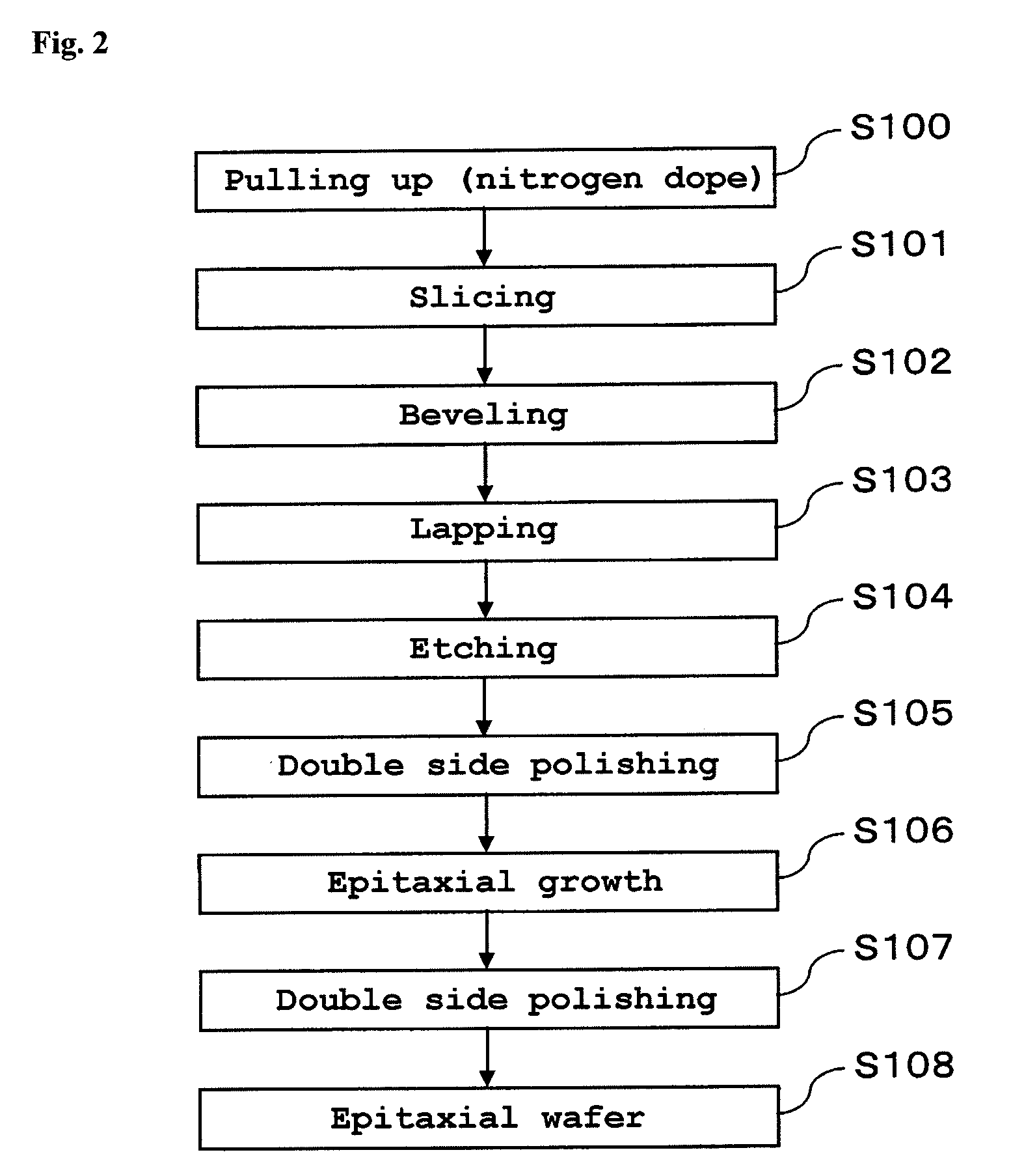
However, as compared with a wafer higher in boron concentration, a wafer

Method used


Image

  • Epitaxial silicon wafer and method for producing the same
  • Epitaxial silicon wafer and method for producing the same
  • Epitaxial silicon wafer and method for producing the same

Examples


Embodiment Construction

[0036]The particulars shown herein are by way of example and for purposes of illustrative discussion of the embodiments of the present invention only and are presented in the cause of providing what is believed to be the most useful and readily understood description of the principles and conceptual aspects of the present invention. In this regard, no attempt is made to show structural details of the present invention in more detail than is necessary for the fundamental understanding of the present invention, the description is taken with the drawings making apparent to those skilled in the art how the forms of the present invention may be embodied in practice. Hereinafter, a description will be given specifically for the example of the present invention.

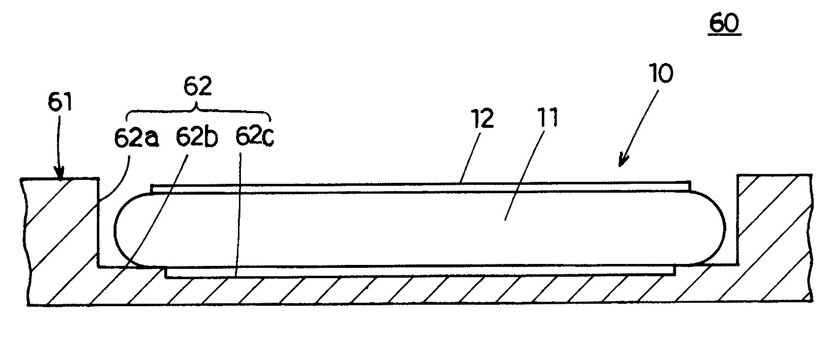
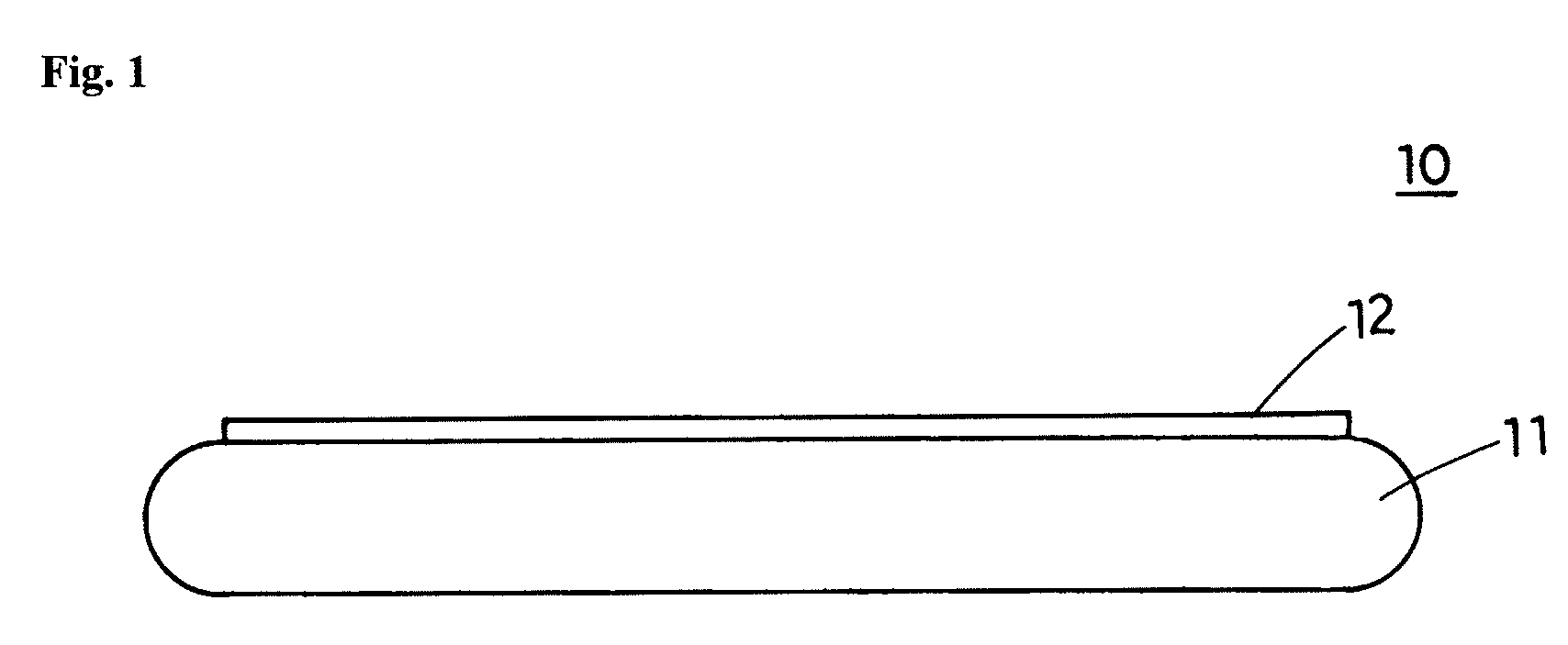
[0037]Referring now to the drawings wherein like characters represent like elements, in FIG. 1, the numeral 10 depicts an epitaxial silicon wafer of the example 1 (i.e., the first example) of the present invention. The epitaxial sil...


PUM


Abstract

An epitaxial silicon wafer in which on growing an epitaxial film only on the front side of a large-sized wafer which is 450 mm or more in diameter, the wafer can be decreased in warpage to obtain a high intrinsic gettering performance and a method for producing the epitaxial silicon wafer. Intrinsic gettering functions have been imparted to a high resistant large-sized silicon wafer which is 450 mm or more in diameter and 0.1 Ω·cm or more in specific resistance by introducing nitrogen, carbon or both of them to a melt on pulling up an ingot. Thereby, after the growth of an epitaxial film, a silicon wafer is less likely to warp greatly. As a result, it is possible to decrease the warpage of an epitaxial silicon wafer and also to obtain a high intrinsic gettering performance.

Description

CROSS-REFERENCE TO RELATED APPLICATIONS[0001]The present application claims priority under 35 U.S.C. §119 of Japanese Application No. 2008-148566 filed on Jun. 5, 2008, the disclosure of which is expressly incorporated by reference herein in its entirety.BACKGROUND OF THE INVENTION[0002]1. Field of the Invention[0003]The present invention relates to an epitaxial silicon wafer having an epitaxial film only on the front side (one side) and a method for producing the epitaxial silicon wafer.[0004]2. Description of the Related Art[0005]Silicon wafers are produced in various steps at which first a single crystal ingot (silicon single crystal) is pulled up by the CZ (Czochralski) method and the ingot is subjected to slicing, beveling, lapping, etching, mirror polishing and washing, for example. However, it is anticipated that as wafers become progressively larger in size, in association with production of the single crystal ingot and silicon wafers, there may be a greater difficulty in pr...

Claims


Application Information

Patent Timeline
IPC IPC(8): H01L21/322B32B3/02
CPCC30B15/02Y10T428/21C30B29/06C30B25/02H01L21/20H01L21/322
Inventor SUGIMOTO, SEIJITAKAISHI, KAZUSHIGE
Owner SUMCO CORP
Why Eureka
Try Eureka