

Semiconductor device and method of manufacturing the same
a semiconductor and semiconductor technology, applied in the direction of semiconductor devices, basic electric elements, electrical equipment, etc., can solve the problem that the phemt is not suitable for the use in the mmic, and achieve the effects of low leakage current, excellent high frequency response characteristics, and high speed operation
- Summary
- Abstract
- Description
- Claims
- Application Information
AI Technical Summary
Benefits of technology
Problems solved by technology
Method used
Image

Examples
first embodiment
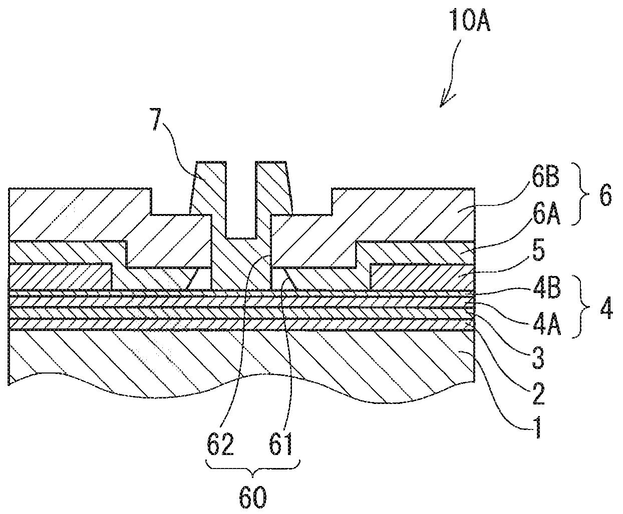
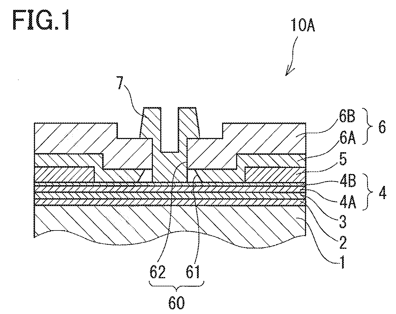
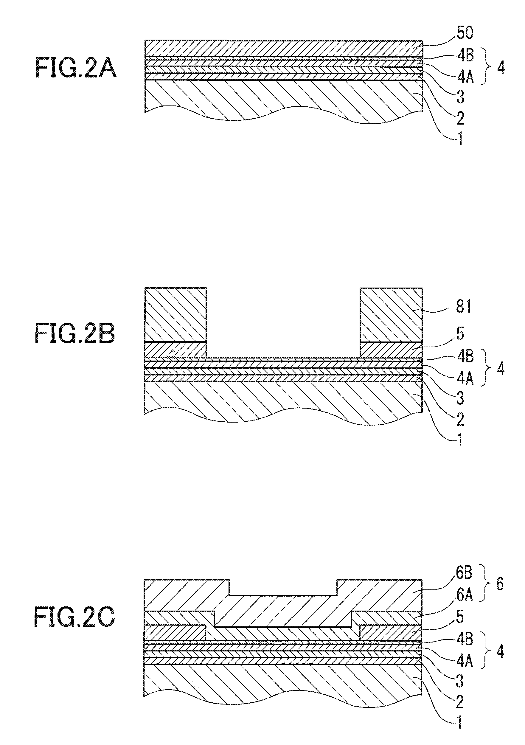
[0028]FIG. 1 is a cross-sectional view of a semiconductor device 10A according to a first embodiment of the present invention. FIGS. 2A to 2C and FIGS. 3A to 3C are diagrams for explaining a method of manufacturing the semiconductor device 10A shown in FIG. 1. The semiconductor device 10A of the present embodiment is a PHEMT, and includes a gate electrode 7, and a source electrode and a drain electrode disposed on opposite sides of the gate electrode 7. It should be noted that the source electrode and the drain electrode are not shown in the diagrams.
[0029]Specifically, the semiconductor device 10A includes: a semi-insulating substrate 1; a buffer layer 2 formed on the semi-insulating substrate 1; a channel layer 3 formed on the buffer layer 2; an electron supply layer 4 formed on the channel layer 3; ohmic contact layers 5 each formed in a predetermined region on the electron supply layer 4; and an insulating film 6 formed on the electron supply layer 4 so as to cover the electron ...
second embodiment
[0045]FIG. 4A is a cross-sectional view of a semiconductor device 10B according to a second embodiment of the present invention. In the second embodiment and the third embodiment to be described later, the same components as those in the first embodiment are designated by the same reference numerals and no further description is given.
[0046]In the semiconductor device 10B, the AlGaAs layer as the first electron supply layer 4A serves as a Schottky layer that forms a Schottky junction with the gate electrode 7, and the InGaP layer as the second electron supply layer 4B is a surface layer that is adjacent to the gate electrode 7. Specifically, the second electron supply layer 4B has an opening 41 having a shape obtained by projecting the shape of the inner peripheral portion 62, which is located on the side opposite to the electron supply layer 4, of the opening 60 in the insulating film 6, on the projected position in the second electron supply layer 4B. The first electron supply lay...
third embodiment
[0048]FIG. 5A is a cross-sectional view of a semiconductor device 10C according to a third embodiment of the present invention. In the semiconductor device 10C, as with the second embodiment, the AlGaAs layer as the first electron supply layer 4A serves as a Schottky layer that forms a Schottky junction with the gate electrode 7. It should be noted, however, that, in the third embodiment, the InGaP layer as the second electron supply layer 4B is a surface layer that is in slight contact with the gate electrode 7. Specifically, in the third embodiment, the opening 41 in the second electron supply layer 4B for exposing the first electron supply layer 4A has a crater shape with its inner peripheral surface being narrowed toward the first electron supply layer 4A. This semiconductor device 10C is manufactured in the following manner.
[0049]First, the insulating film 6 is formed and then the opening 60 is formed in the insulating film 6 by dry etching in the same manner as in the first em...
PUM
 Abstract
Description
Claims
Application Information