

Techniques for Enhancing Performance of Photovoltaic Devices
- Summary
- Abstract
- Description
- Claims
- Application Information
AI Technical Summary
Benefits of technology
Problems solved by technology
Method used
Image

Examples
example 1
[0035]This example uses spin-coating as a deposition technique to demonstrate the differences between CIGS thin films prepared with and without Sb-doping. In particular, the grain size enhancement effect upon the addition of Sb will be illustrated (at two temperature sets, 350° C. and 400° C.). The effects of Sb on CuInSe2 (CIS), the Ga-free analogue of CIGS, were described in U.S. patent application Ser. No. 11 / 951,858, filed by Mitzi et al., entitled “Improved Photovoltaic Device with Solution-Processed Chalcogenide Absorber Layer,” the contents of which are incorporated by reference herein.
[0036]The solutions used for the thin-film deposition were prepared in an inert atmosphere in two steps. First, a solution was prepared for each individual component metal chalcogenide, at room temperature. Next, these component solutions (some with and some without the Sb component) were mixed in appropriate ratios to yield a stoichiometric solution for a targeted overall CIGS composition, see...
example 2
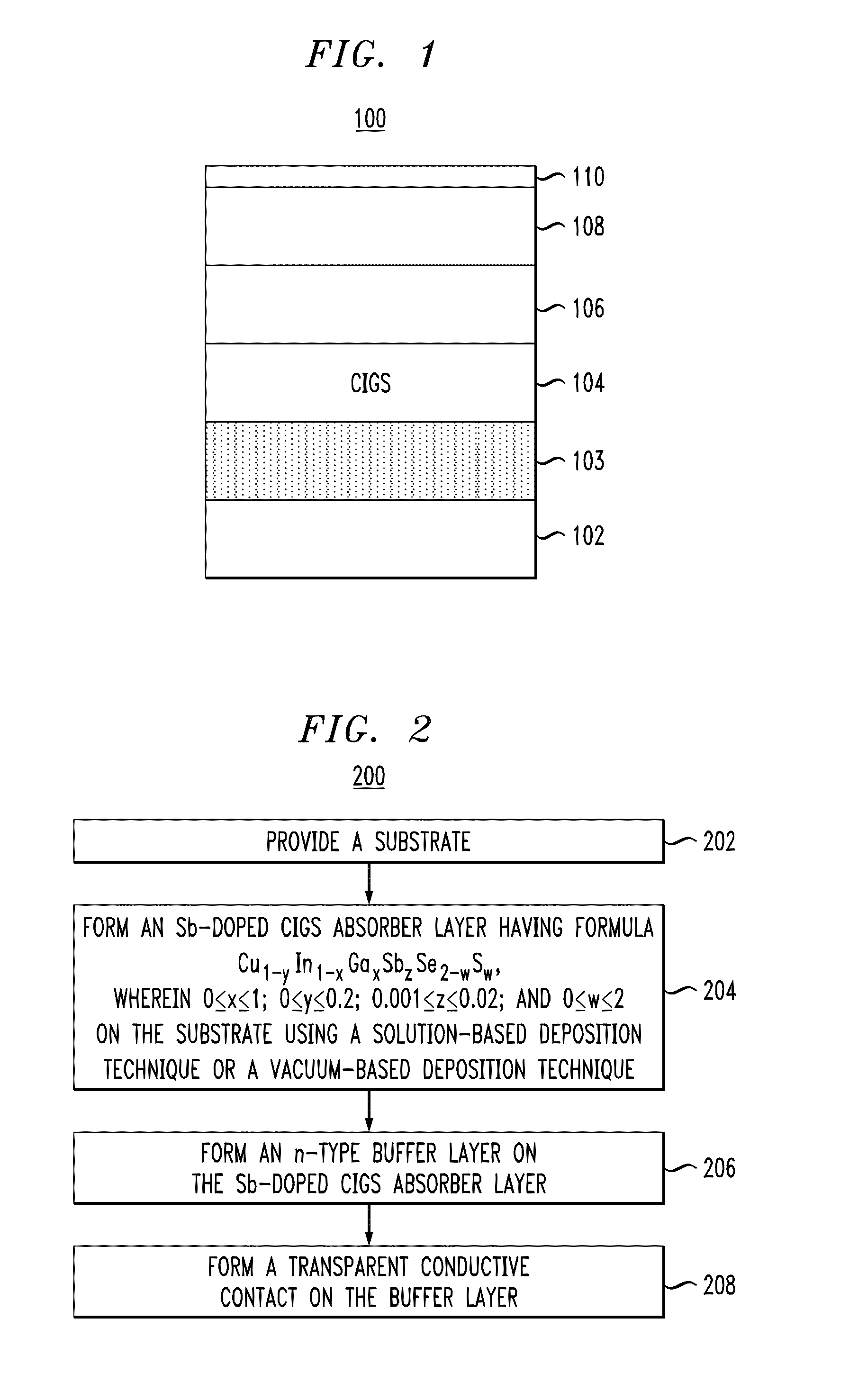
[0055]The CIGS absorber layers described above were incorporated into two working photovoltaic devices having the structure of photovoltaic device 100, described in conjunction with the description of FIG. 1, above, with the CIGS absorber layers deposited using the spin-coating method described in Example 1 (above), containing zero or 0.2 mol % of Sb dopant, respectively. The CIGS layers were annealed at 525° C. for 15 minutes as final heat treatments. A one inch×one inch soda-lime glass plate (0.04 inch thickness) with about 600 nm of Mo sputtered thereon formed the back contact of the device.
[0056]For each component solution, the solid components were weighed and the solutions were formed in a nitrogen-filled glove box with water and oxygen levels maintained below one part per million (ppm). Five component solutions, i.e., component solutions (a)-(e) for the CIGS absorber layer were prepared by dissolving a Cu source, an In source, a Ga source, an Se source and an Sb source in hyd...
example 3
[0067]This example illustrates a working CIGS photovoltaic device fabricated in a same manner as described in conjunction with the description of Example 2, above, containing a small amount of Sb dopants, and processed at a relatively low temperature (375° C. maximum temperature). A one inch×one inch soda-lime glass plate (0.04 inch thickness) with about 600 nm of Mo sputtered thereon formed a back contact of the device.
[0068]For each component solution, the solid components were weighed and the solutions were formed in a nitrogen-filled glove box with water and oxygen levels maintained below one ppm (as for the other examples). Five component solutions, i.e., component solutions (a)-(e), for the CIGS layer were prepared by dissolving a Cu source, an In source, a Ga source, an Se source and an Sb source in hydrazine as follows.
[0069]Component solution (a) (Cu2S) was formed by mixing 10 mmol Cu2S (1.592 g), 20 mmol S (0.6413 g) and 20.0 mL of anhydrous hydrazine (Aldrich, anhydrous, ...
PUM
| Property | Measurement | Unit |
|---|---|---|
| Grain size | aaaaa | aaaaa |
| Grain size | aaaaa | aaaaa |
| Grain size | aaaaa | aaaaa |
Abstract
Description
Claims
Application Information