
Fabrication of compact opto-electronic component packages

a technology of optoelectronic components and components, applied in the direction of electrical equipment, semiconductor devices, semiconductor/solid-state device details, etc., can solve the problems of large footprint, difficult application-specific designs, poor thermal conductivity and large mechanical tolerances, etc., to achieve greater design flexibility, easy incorporation into manufacturing processes, and better thermal isolation or performance

Inactive Publication Date: 2009-12-31
EPISTAR CORP
View PDF6 Cites 17 Cited by
  • Summary
  • Abstract
  • Description
  • Claims
  • Application Information

AI Technical Summary

Benefits of technology

[0010]Some implementations result in smaller or thinner packages that provide better thermal isolation or performance and can provide for greater design flexibility which allows for changes to the design to be easily incorporated into a manufacturing process. In addition, various modifications to the process can be made such that the process can be used with a LED or other opto-electronic component package with an integrated electronic circuit structure.

Problems solved by technology

These types of packages often have large footprints, poor thermal conductivity and large mechanical tolerances and are not flexible to design changes, thus making application-specific designs difficult.

Method used


Image

  • Fabrication of compact opto-electronic component packages
  • Fabrication of compact opto-electronic component packages
  • Fabrication of compact opto-electronic component packages

Examples


Embodiment Construction

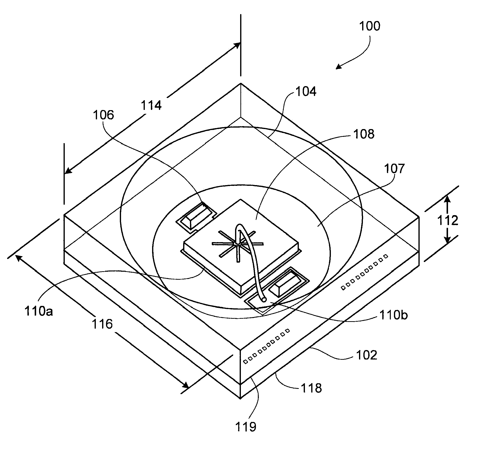
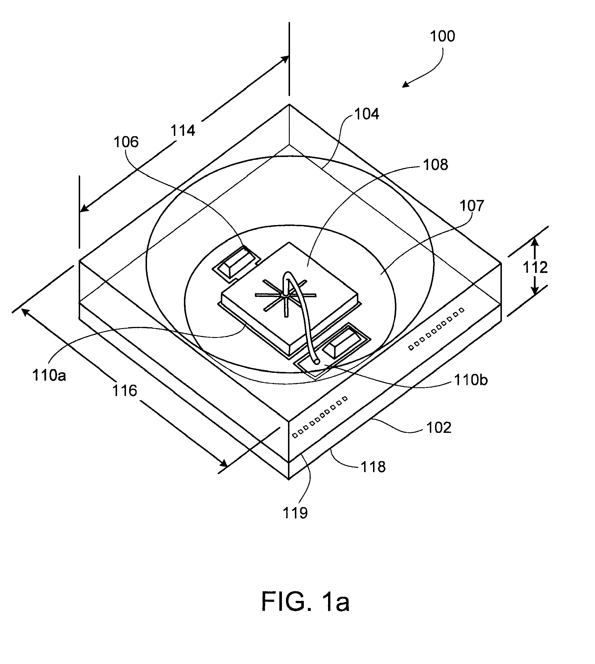
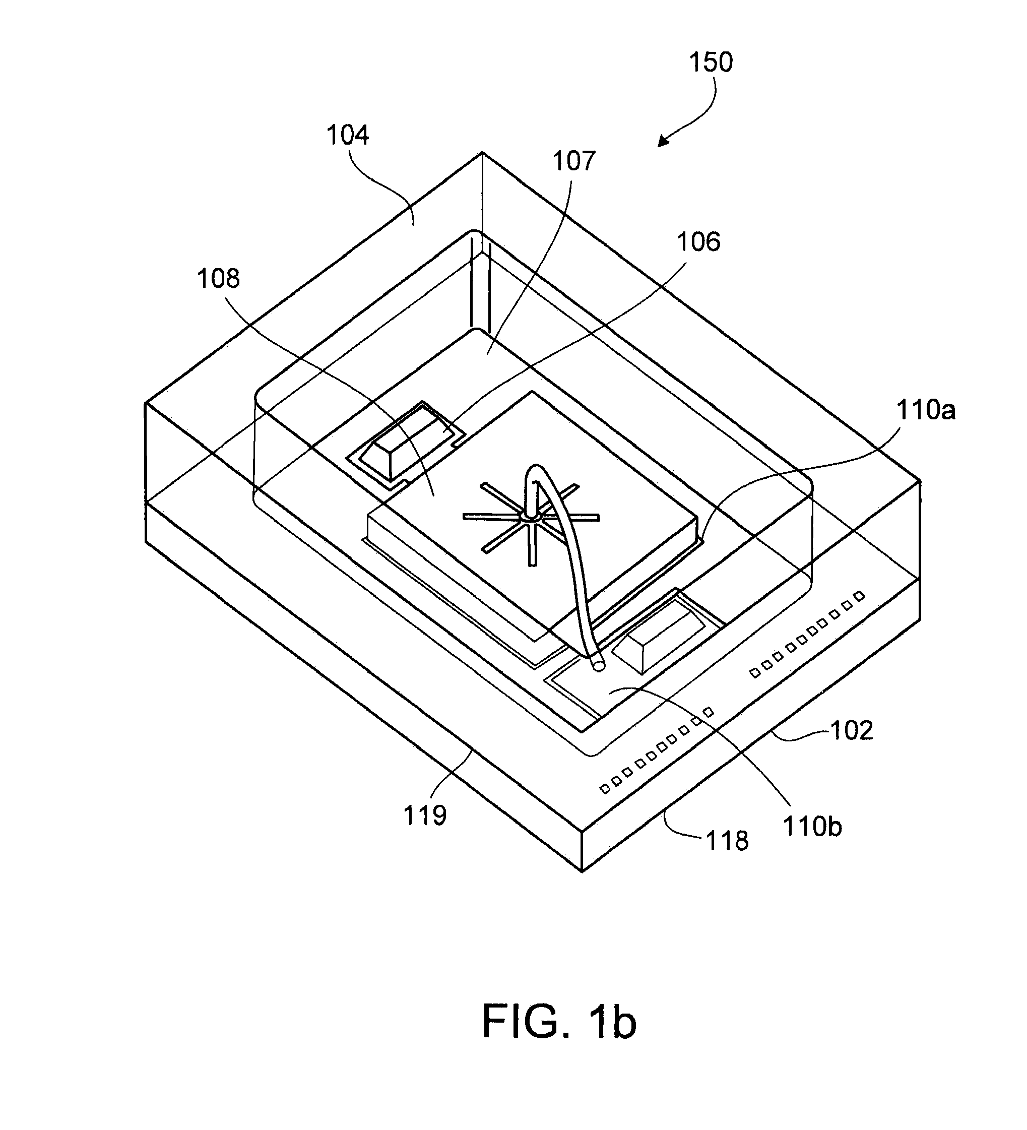
[0032]FIGS. 1a and 1b illustrate examples of thin LED packages 100 and 150 with enhanced thermal performance 100 and 150. Although FIGS. 1a and 1b are described with respect to a LED 108, the LED 108 can be replaced with other types of opto-electronic components. For example, in some implementations, the LED 108 is replaced by an infra-red emitter (e.g., a vertical-cavity surface-emitting laser), an infra-red receiver (e.g., a pin diode) or an infra-red transceiver. Likewise, the fabrication processes described below can be used to make packages for opto-electronic components other than LEDs.

[0033]The LED package 100 includes a base 102, a reflector 104, feed-through metallization 106, a reflective surface 107, an LED 108, a LED die attach pad 110a (located underneath the LED 108) and wirebond pads 110b. In the illustrated example, the base 102 is formed from a silicon or other semiconductor wafer. The physical dimensions (e.g., the height 112, the width 114 and the depth 116) of th...


PUM


Abstract

A wafer-level method of fabricating an opto-electronic component package, in which the opto-electronic component is mounted to a semiconductor wafer having first and second surfaces on opposite sides of the wafer. The method includes etching vias in the first surface of the semiconductor wafer. The first surface and surfaces in the vias are metallized, and the metal is structured to define a thermal pad and to define the anode and cathode contact pads. A carrier wafer is attached on the side of the semiconductor wafer having the first surface, and the semiconductor wafer is thinned from its second surface to expose the metallization in the vias. Metal is provided on the second surface, and the metal is structured to define a die attach pad and additional anode and cathode pads for the opto-electronic component. The opto-electronic component is mounted on the die attach pad and a protective cover is formed over the opto-electronic component.

Description

CROSS-REFERENCE TO RELATED APPLICATION(S)[0001]This application claims the benefit of priority of U.S. Provisional Patent Application 61 / 076,263, filed on Jun. 27, 2008, the contents of which are incorporated by reference in its entirety.TECHNICAL FIELD[0002]This invention relates to opto-electronic component packages.BACKGROUND[0003]The use of light emitting diodes (LEDs) in electronic products is ever-increasing and in some cases are replacing traditional light sources, such as light bulbs, in existing applications. For example, LEDs can now be found in flashlights, automotive headlights and backlight units for LCD screens.[0004]Ceramics such as alumina oxide (Al2O3) or aluminum nitride (AlN) are used in the packaging of high brightness LEDs. In addition to ceramics, plastic leadless chip carriers (“PLCC”) and other leadframe configurations are also used. These types of packages often have large footprints, poor thermal conductivity and large mechanical tolerances and are not flex...

Claims


Application Information

Patent Timeline
Patent Type & Authority Applications(United States)
IPC IPC(8): H01L21/50H01L33/00H01L33/38H01L33/48H01L33/62
CPCH01L21/76898H01L2224/73265H01L33/486H01L33/62H01L2224/48091H01L2224/48227H01L2224/48465H01L2933/0016H01L23/481H01L2924/10253H01L2924/12041H01L2924/3025H01L24/48H01L2924/01019H01L2924/00014H01L2924/00H01L2924/14H01L2924/181H01L2224/45099H01L2224/45015H01L2924/207
Inventor KUHMANN, JOCHEN
Owner EPISTAR CORP
Learn More