Photovoltaic Modules Manufactured Using Monolithic Module Assembly Techniques

a technology of solar cells and modules, applied in photovoltaics, electrical equipment, semiconductor devices, etc., can solve the problems of difficult automation of electrically connecting solar cells in series, high cost, limited throughput of stringers/tabbers,

Inactive Publication Date: 2010-01-21
APPLIED MATERIALS INC
View PDF100 Cites 162 Cited by
  • Summary
  • Abstract
  • Description
  • Claims
  • Application Information

AI Technical Summary

Benefits of technology

[0022]The electrical circuit on the backsheet can cover nearly the entire surface. The conductivity of the electrical interconnects can thus be very large because the interconnect is much wider. Meanwhile, the wider conductor can be made thinner (typically less than 100 μm) and still have low resistance. The thin conductor is typically more flexible than Cu ribbon interconnects, thereby reducing stress.

Problems solved by technology

Limitations of this process include the following:The process of electrically connecting solar cells in series is difficult to automate so that stringer / tabbers have limited throughput and are expensive.The assembled solar cell circuit is very fragile prior to the lamination step.The Cu ribbon interconnect must be narrow to avoid reflecting too much light, and can not be very thick or it becomes too stiff and stresses the cell.
The net result is that the conductivity of the Cu interconnect is limited and the electrical losses due to the interconnect are large.The above limitations make this process difficult to use with thin crystalline-silicon solar cells.
Use of thinner Si reduces the cost of the solar cell.The spacing between solar cells must be large enough to accommodate stress relief for the Cu interconnect wire, which reduces the module efficiency due to the non-utilized space between solar cells.The process comprises many steps, thus increasing the manufacturing cost.
This is unlike stringer / tabbers where additional Cu interconnect straps or contacting points increase cost.

Method used


Image

  • Photovoltaic Modules Manufactured Using Monolithic Module Assembly Techniques
  • Photovoltaic Modules Manufactured Using Monolithic Module Assembly Techniques
  • Photovoltaic Modules Manufactured Using Monolithic Module Assembly Techniques

Examples


Embodiment Construction

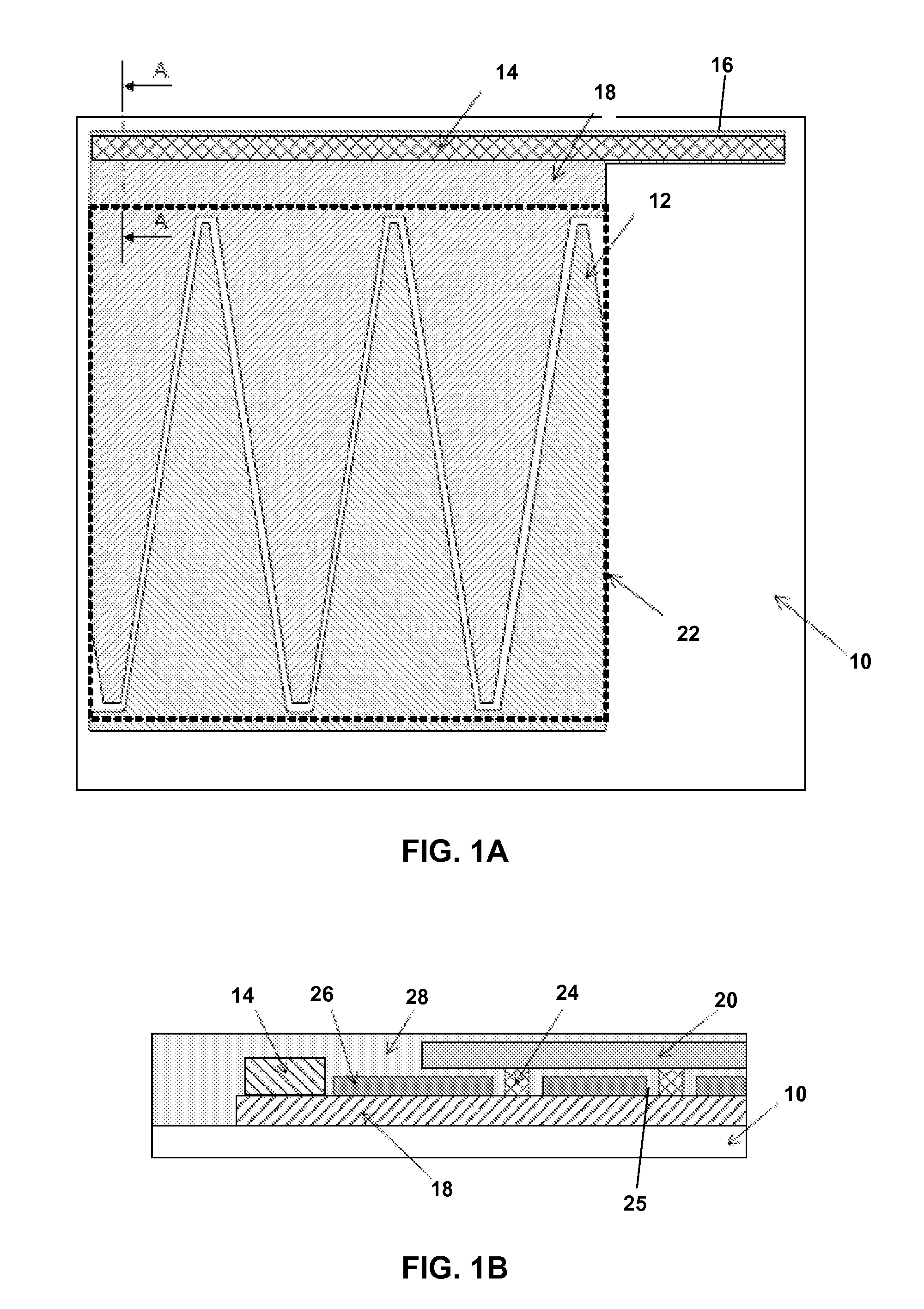
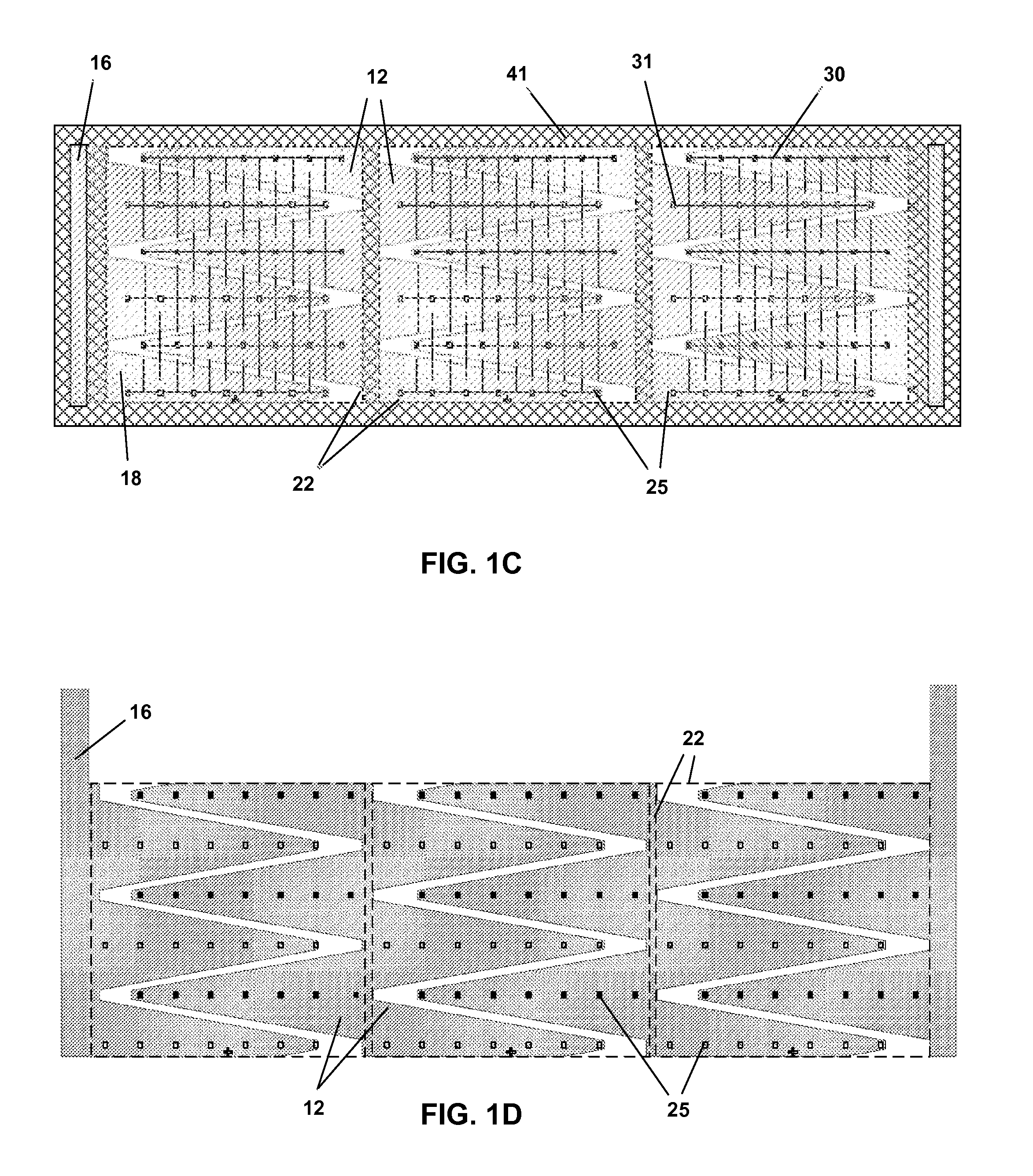
Monolithically Integrated Cu Bussing

[0048]As used throughout the specification and claims, the term “bus” means a bus bar, bus ribbon, bus strap, or any other conductive element suitable for current bussing.

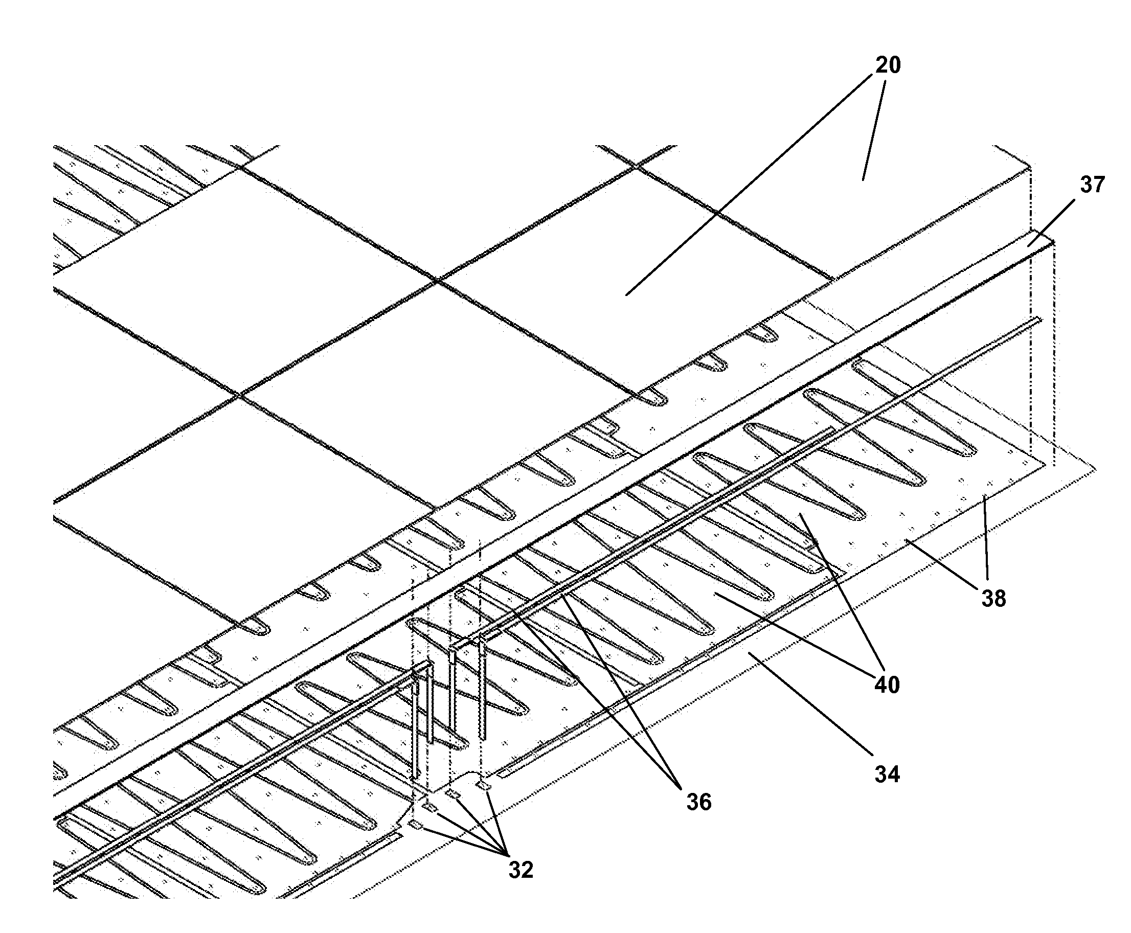
[0049]In photovoltaic modules using conventional cells, the solar cell strings are terminated at the top and bottom of the module using copper (Cu) bus straps. These Cu bus straps are often coated with Sn or Sn / Ag to prevent interaction with the encapsulant and to enhance solderability. The current needs to be transported a long distance (up to half the width of the photovoltaic module) to the junction box in the center of the module. The Cu bus straps need a large cross sectional area to have sufficiently low resistance to transport current such a long distance with low resistance losses.

[0050]In monolithic module assembly, shown in FIGS. 1A-1D, the solar cells are preferably interconnected using thin metal metallizations or foils 12, 18 of opposite polarity (preferably comprisi...


PUM


Abstract

Photovoltaic modules comprising back-contact solar cells manufactured using monolithic module assembly techniques comprising a flexible circuit comprising a back sheet and a patterned metallization. The module may comprise busses in electrical contact with the patterned metallization to extract the current. The module may alternatively comprise multilevel metallizations. Interlayer dielectric comprising islands or dots relieves stresses due to thermal mismatch. The use of multiple cord plates enables flexible circuit layouts, thus optimizing the module. The modules preferably comprise a thermoplastic encapsulant and / or hybrid adhesive / solder materials. An ultrathin moisture barrier enables roll-to-roll processing.

Description

CROSS-REFERENCE TO RELATED APPLICATIONS[0001]This application claims the benefit of the filing of U.S. Provisional Patent Application Ser. No. 61 / 048,898, entitled “Photovoltaic Modules using Monolithic Module Assembly”, filed on Apr. 29, 2008, and U.S. Provisional Patent Application Ser. No. 61 / 093,673, entitled “Photovoltaic Modules using Monolithic Module Assembly Techniques”, filed on Sep. 2, 2008, and the specifications thereof are incorporated herein by reference.BACKGROUND OF THE INVENTION[0002]1. Field of the Invention (Technical Field)[0003]The present invention comprises methods for manufacturing solar cell modules using monolithic module assembly configurations and methods.[0004]2. Description of Related Art[0005]Note that the following discussion refers to a number of publications by author(s) and year of publication, and that due to recent publication dates certain publications are not to be considered as prior art vis-à-vis the present invention. Discussion of such pub...

Claims


Application Information

Patent Timeline
Patent Type & Authority Applications(United States)
IPC IPC(8): H01L31/048H01L31/042
CPCH01L31/048Y02E10/50H02S40/34H01L31/02013H01L31/0516H01L31/0201H01L31/049
Inventor MEAKIN, DAVID H.GEE, JAMES M.SOUTHIMATH, SYSAVANHMURPHY, BRIANTELLE, JOHNMITCHELL, ANDREW MARK
Owner APPLIED MATERIALS INC
Why Eureka
Try Eureka