
Method and apparatus for simultaneous lateral and vertical patterning of molecular organic films

a technology of molecular organic thin films and simultaneous lateral and vertical patterning, which is applied in the direction of applications, manufacturing tools, instruments, etc., can solve the problems of limited resolution, difficult to make large area shadow masks, and limited techniques, and achieves greater lift-off thickness and weaker intermolecular bonds

Inactive Publication Date: 2010-02-11
MASSACHUSETTS INST OF TECH
View PDF14 Cites 9 Cited by
  • Summary
  • Abstract
  • Description
  • Claims
  • Application Information

AI Technical Summary

Benefits of technology

[0010]The invention relates to a method for fabricating a large area OLED structure which can produce features smaller than 30 μm without heating or applying pressure to the organic layer. A proxy for the intermolecular bonding strength is the sublimation temperature ...

Problems solved by technology

A challenge in fabricating OLEDs is patterning micron-sized features of molecular organic thin films over large areas.
This technique is limited in resolution due to lateral diffusion from the spacing between the shadow mask and the substrate and the thickness of the shadow mask.
Experience shows that it is difficult to make large area shadow masks with features smaller than 150 μm.
LITI and LIPS rely on thermal transfer of organic layer and are limited in resolution due to the ability to focus the laser.
MoJet uses a Micro-Electro-Mechanical System (“MEMS”) valve to pattern the organic layer and is not limited in resolution, but the valve is susceptible to clogging.
Large area scalability of these techniques requires multiple lasers or MEMS valves which is both costly and labor intensive.
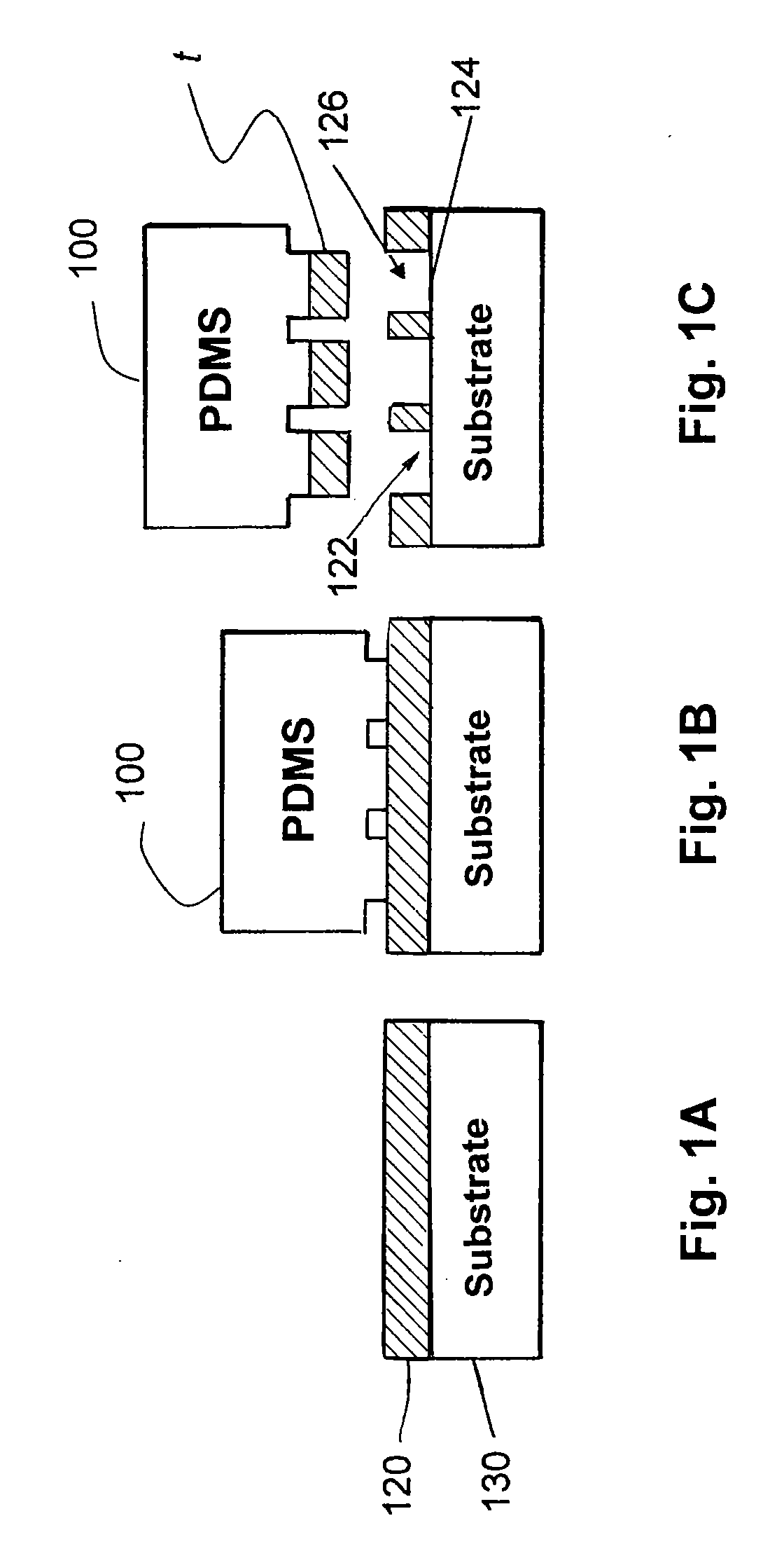
However, conventional contact stamping requires elevated temperature and pressure which are unsuited for OLED fabrication.
Heat and pressure can be detrimental to certain organic material used in the OLED as they can cause contamination or alteration of the organic component.

Method used


Image

  • Method and apparatus for simultaneous lateral and vertical patterning of molecular organic films
  • Method and apparatus for simultaneous lateral and vertical patterning of molecular organic films
  • Method and apparatus for simultaneous lateral and vertical patterning of molecular organic films

Examples


experiment 1

Fabrication of OLEDs

[0057]Glass substrates are cleaned using a mixture of a cleaning solution and water, rinsed and sonicated with de-ionized water, acetone and boiling isopropanol and then treated with 5 minutes of oxygen plasma before spin coating. PEDOT:PSS was spin coated at 10° C. ramp and 3000 rpm for 30 seconds and subsequently baked for 10 minutes at 150° C. on a hotplate with glass dish cover. The samples were moved into a nitrogen glove box for organic deposition. Thermal evaporation of the organic layers occurred at pressures lower than 5×10⁻⁶ Torr, and deposition of organic layers ranged 1-5 A / s. The organic lift-off procedure was also performed in the nitrogen glove box on one of the two devices. After patterning, the device was completed by depositing the remaining organic layer and electrode cap of 50 nm Mg:Ag (10:1 weight ratio) / 50 nm Ag.

[0058]The PDMS stamp consists of a 10:1 weight ratio of base to curing agent from a Silicone Elastomer Kit. The mixture was stirred...

experiment 2

Fabrication of OLEDs

[0063]Several OLEDs were fabricated on ITO-coated glass substrates by first cleaning the substrate with sonication and then rinsing with de-ionized water, acetone, and boiling isopropanol. The substrates were treated by exposure to oxygen plasma for about five minutes. PEDOT:PSS was spin coated at 10° K. ramp and 3000 rpm for 30 seconds and subsequently baked for 10 minutes at 150° C. on a hotplate with glass dish cover. The samples were moved into a nitrogen glove box from where they were loaded into an integrated organic deposition vacuum chamber. A 50 nm thick TPD film and 20 nm thick TAZ film were thermally evaporated at base pressure of less than 5×10⁻⁶ Torr. Substrates were transferred back into the nitrogen-filled glove box where they were patterned using the stamp lift-off technique. Following the patterning step, the devices were coated with a 50 nm thick film of aluminum-tris-quinolate (Alq3), the electrode cap of 50 nm thick Mg:Ag (10:1 weight ratio) a...

experiment 3

Large Scale Fabrication

[0066]To evaluate suitability of the CLOP technique in fabrication of OLEDs, a set of OLEDs with blanket deposited organic films was compared to a set of OLEDs in which the lift-off patterning was applied to remove partial thickness of the hole transport layer. To avoid variation in the quality of the organic thin films, both devices were grown simultaneously on the same substrate.

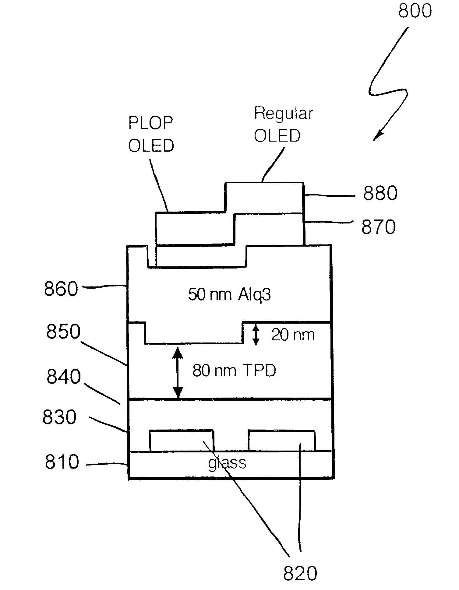
[0067]FIG. 8A schematically illustrates the device patterned according to the disclosed embodiments. Namely, device 800 of FIG. 8 includes substrate 810, supporting ITO electrodes 820 and layer 830 which comprises PEDOT:PSS. TPD layer 840 had an initial thickness of about 100 nm. Using the disclosed patterning technique a portion of the TPD layer 840 has been patterned to form a via 20 nm deep. Layer 850 is Alq3 and is about 50 nm thick. The final structure has a common Mg:Ag cathode (layer 860) and independent ITO (layer 870) cathode. Other than the nm via, the base line device had ...


PUM

PropertyMeasurementUnit
Depthaaaaaaaaaa
Temperatureaaaaaaaaaa
Pressureaaaaaaaaaa

Abstract

The disclosure relates to a method and apparatus for micro-patterning organic layers of OLEDs. The disclosed methods do not require applying pressure to the film, nor do they require heat treatment, surface treatment or fast release rate of a stamp from the substrate. The disclosed methods are particularly advantageous over the conventional shadow masking techniques for providing large array fabrication with small features. In one embodiment of the disclosure, one or more organic films are selected for the OLED as a function of their individual or combined sublimation temperature. The material is selected in view of the depth and shape of the features that are to be formed in the organic layer. The disclosed embodiments can provide minimum feature size of 13 μm which is suitable for high resolution OLED displays.

Description

CROSS-REFERENCE TO RELATED APPLICATIONS[0001]This application claims the benefit of U.S. provisional patent application No. 61 / 087,088, filed Aug. 7, 2008 for Simultaneous Lateral and Vertical Patterning of Molecular Organic Thin Films Via Microcontact Lift-off Applied to Fabrication of Organic Light Emitting Device Arrays, the entire subject matter of which is incorporated herein.BACKGROUND[0002]1. Field of the Invention[0003]The disclosure generally relates to method and apparatus for simultaneous lateral and vertical patterning of molecular organic thin films via microcontact patterning. The disclosed process can be applied to fabrication of organic light emitting device arrays and has been found particularly advantageous over the conventional techniques in that large arrays can be formed without cost constraints of the conventional techniques.[0004]2. Description of Related Art[0005]Organic light emitting devices (OLEDs) are thin, brightly emissive and efficient diodes which hav...

Claims


Application Information

Patent Timeline
IPC IPC(8): H01L51/54H01L51/40H01L51/56B28B21/42
CPCH01L51/0019H01L51/50H01L51/0059H01L51/0037H10K71/236H10K85/1135H10K85/631H10K50/00
Inventor BULOVIC, VLADIMIRYU, JENNIFER J.
Owner MASSACHUSETTS INST OF TECH
Learn More