Method for fabricating mos transistors

a transistor and mos technology, applied in the direction of transistors, semiconductor devices, electrical equipment, etc., can solve the problems of affecting the operation of the device, so as to improve the salicide piping and agglomeration

Active Publication Date: 2010-02-11
UNITED MICROELECTRONICS CORP
View PDF5 Cites 9 Cited by
  • Summary
  • Abstract
  • Description
  • Claims
  • Application Information

AI Technical Summary

Benefits of technology

[0012]The present invention specifically conducts a cleaning process to fully remove native oxides from the surface of the semiconductor substrate before the salicide process is performed, and conducts an oxidation process thereafter to form an oxide layer over the surface of the semiconductor substrate. This oxide layer is later treated with fluorine-containing plasma to transform into a fluorine-containing layer, and a salicide process is conducted thereafter. As the fluorine atom embedded within the fluorine-containing layer could be used to prevent silicide metal formed thereafter from being too close to the channel region and also protect silicide from high temperature of degassing process, problems such as salicide piping and agglomeration can be improved significantly.

Problems solved by technology

Nevertheless, the interconnection between the contact plugs and the silicon material of the gate structure and the source / drain region is usually poor, hence a silicide material is often formed over the surface of the gate structure and the source / drain region to improve the ohmic contact between the contact plugs and the gate structure and the source / drain region.
However, when the silicides are being formed, the atoms within the metal layer will diffuse into the substrate and deplete the silicon within the source / drain region, thereby damaging the original lattice structure of the source / drain region and causing the PN junction between the source / drain region and the silicon substrate to react with the silicon contained within the source / drain region as a result of an overly short distance between the PN junction and the silicide layer.
Ultimately, the problems become much worse in the design of ultra shallow junctions (USJ) as the silicides often come in contact directly with the substrate and result in failure of the device.
On the other hand, if the depth of the silicides is kept constant, the distance between the PN junction of the source / drain region 72 and the silicon substrate and the silicide layer 76 may become overly short and result in junction leakage.
Additionally, the mixture utilized during the wet cleaning process will corrode the liner disposed between the gate electrode and the spacer and cause the silicide to approach the channel area during silicide formation and result in a nickel silicide piping phenomenon.
Moreover, due to high temperature of the PVD chamber or the degas process, the as-deposition formed before the rapid thermal annealing process will result in silicides with polycrystalline structure and degrade the overall thermal stability.
In other words, when the treatment temperature is too high or process time of the treatment is too long, the silicides will become pieces of unconnected mass and result in an agglomeration phenomenon and increase the sheet resistance.
Additionally, a high temperature will induce a conversion and consume silicon excessively, and cause a spiking phenomenon in the ultra shallow junction or forming a high resistivity structure, such as converting the low resistivity state nickel silicide (NiSi) having less than 20 μΩ-cm to a high resistivity state nickel disilicide (NiSi2) having approximately 50 μΩ-cm.

Method used


Image

  • Method for fabricating mos transistors
  • Method for fabricating mos transistors
  • Method for fabricating mos transistors

Examples


Embodiment Construction

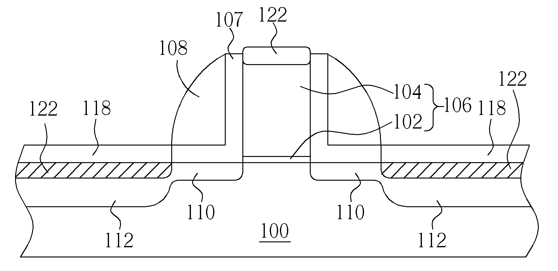
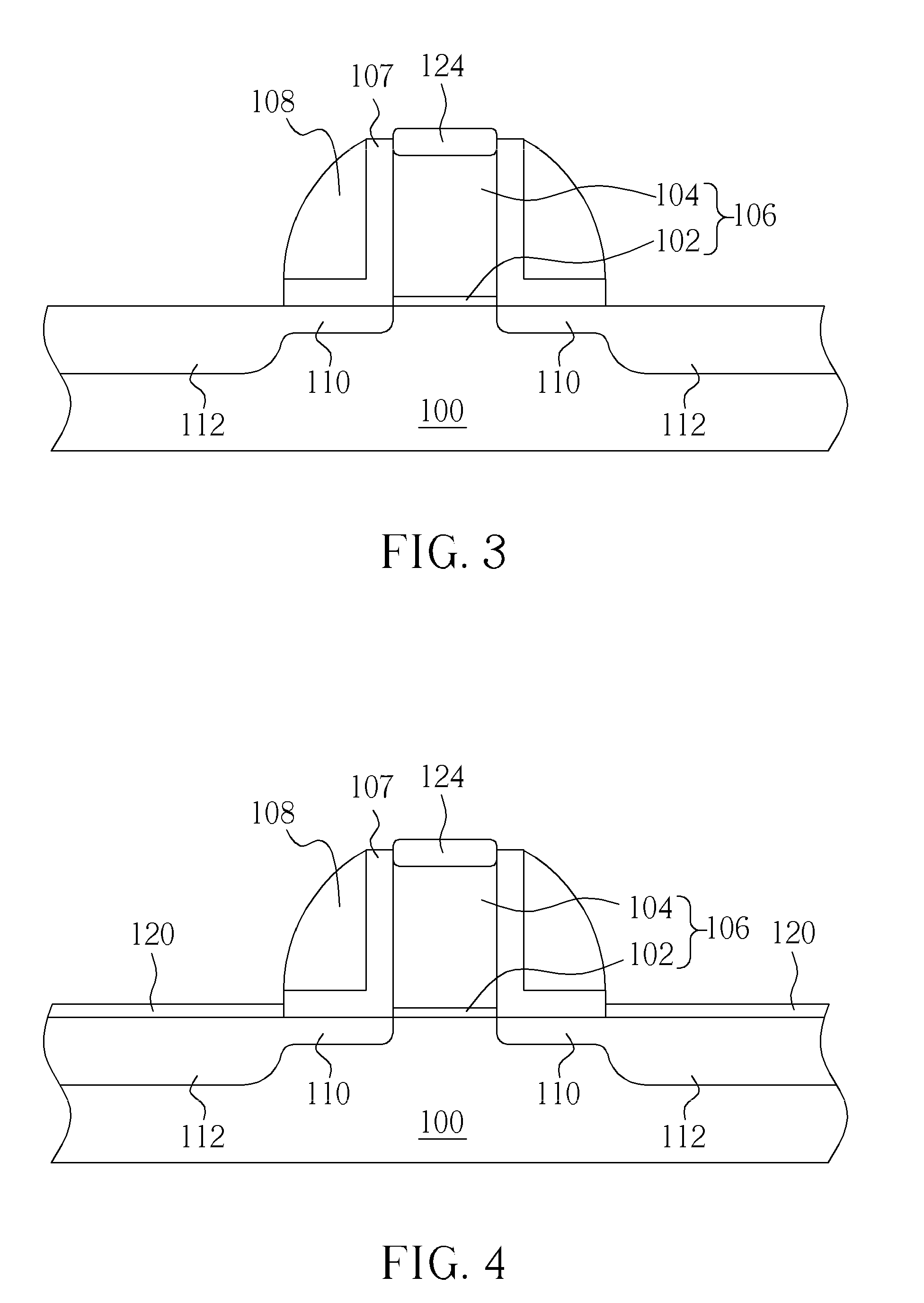
[0016]Referring to FIGS. 3-7, FIGS. 3-7 illustrate a method for fabricating a MOS transistor according to a preferred embodiment of the present invention. As shown in FIG. 3, a substrate 100, such as a wafer or a silicon-on-insulator (SOI) substrate is provided. Preferably, the semiconductor substrate 100 may include structures such as gates, source / drain regions, isolation regions, word lines, or resistors depending on different product demands and fabrication processes. According to the preferred embodiment of the present invention, a gate structure and source / drain region of a MOS transistor are utilized as an example, as shown in FIGS. 3-7. As shown in FIG. 3, the gate structure 102 includes a gate dielectric layer 102 and gate conductive layer 104. The gate dielectric layer 102 is preferably composed of insulating material such as silicon nitrides, oxides, oxynitrides, or metal oxides, and the gate conductive layer 104 is composed of conductive material such as doped polysilico...


PUM


Abstract

A method for fabricating metal-oxide transistors is disclosed. First, a semiconductor substrate having a gate structure is provided, in which the gate structure includes a gate dielectric layer and a gate. A source/drain region is formed in the semiconductor substrate, and a cleaning step is performed to fully remove native oxides from the surface of the semiconductor substrate. An oxidation process is conducted to form an oxide layer on the semiconductor substrate and the oxide layer is then treated with fluorine-containing plasma to form a fluorine-containing layer on the surface of the semiconductor substrate. A metal layer is deposited on the semiconductor substrate thereafter and a thermal treatment is performed to transform the metal layer into a silicide layer.

Description

BACKGROUND OF THE INVENTION [0001]1. Field of the Invention[0002]The invention relates to a method for fabricating MOS transistors, and more particularly, to a method for fabricating a fluorine-containing layer before performing a salicide process.[0003]2. Description of the Prior Art[0004]Field effect transistors are important electronic devices in the fabrication of integrated circuits, and as the size of the semiconductor device becomes smaller and smaller, the fabrication of the transistors also improves and is constantly enhanced for fabricating transistors with smaller sizes and higher quality.[0005]In the conventional method of fabricating transistors, a gate structure is first formed on a substrate, and a lightly doped drain (LDD) is formed on the two corresponding sides of the gate structure. Next, a spacer is formed on the sidewall of the gate structure and an ion implantation process is performed to form a source / drain region within the substrate by utilizing the gate str...

Claims


Application Information

Patent Timeline
Patent Type & Authority Applications(United States)
IPC IPC(8): H01L21/336
CPCH01L21/28518H01L29/66636H01L29/6659H01L29/165
Inventor LAI, KUO-CHIHCHEN, YI-WEIHO, NIEN-TINGTSAI, TENG-CHUN
Owner UNITED MICROELECTRONICS CORP
Why Eureka
Try Eureka