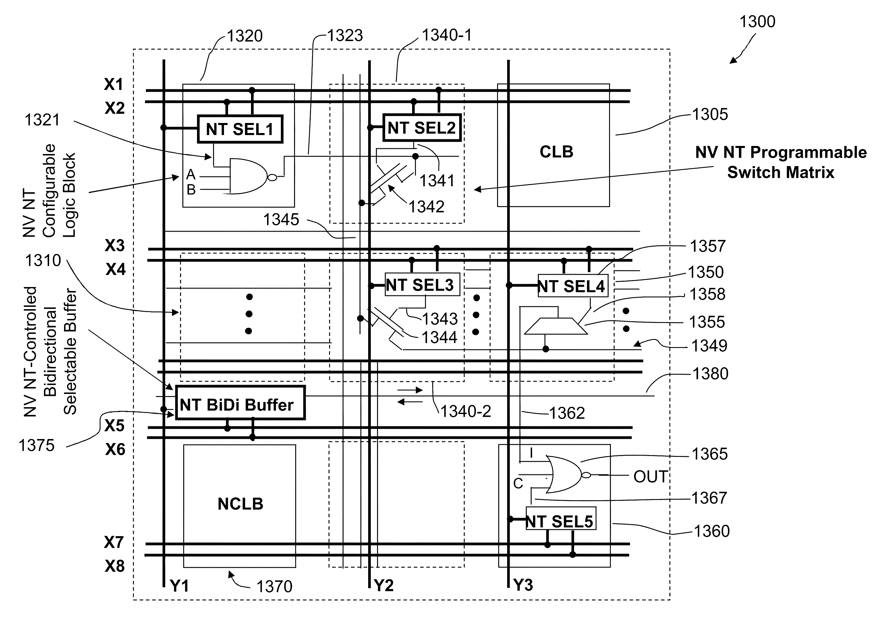
[0045]Under certain embodiments, one or more nonvolatile
nanotube (NV NT) select circuits are used to store (in a first operation) and later provide (in a second operation) one or more control bits to a conventional configurable
logic block (CLB) circuit. Said NV NT select circuits comprise a pair of
nanotube switches and a
field effect transistor (FET). One terminal of each nanotube switch and one terminal of the FET are joined together to form a common node, providing a four terminal device. During a store operation, the resistance of each nanotube switch can be set to provide means for nonvolatile storage of a single control bit. During NFPGA operation, the control bits stored as corresponding nonvolatile high or
low resistance states within each NV NT select circuit can be readily accessed and used to configure the CLB circuit. This nonvolatile nanotube based CLB
system is referred to as an NCLB.
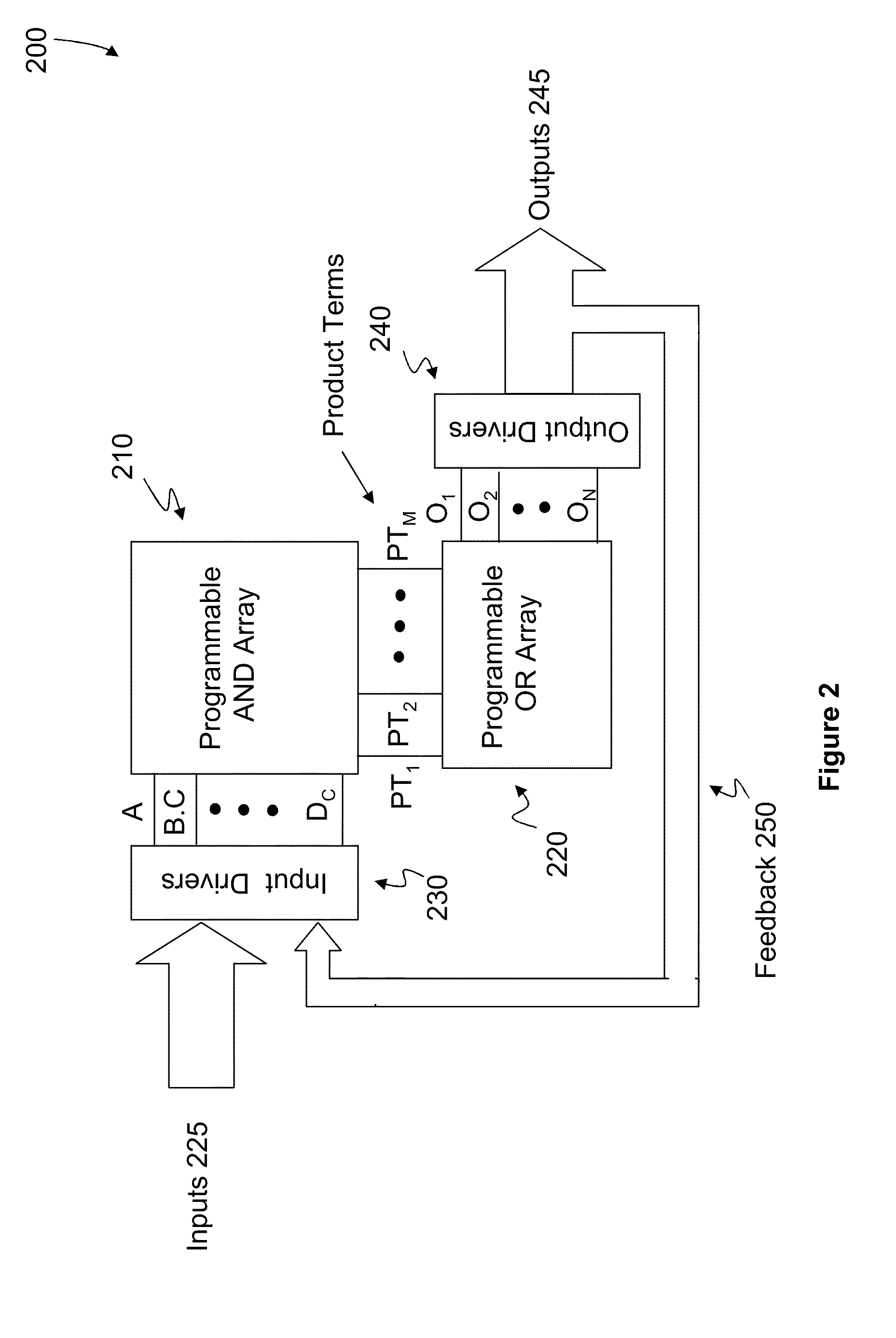
[0048]Under certain embodiments, a plurality of nonvolatile NRAM™ cells are combined to form an NRAM™ array, providing means for nonvolatile storage of a plurality of
data bits, each data bit corresponding to a unique combination of inputs (address) to the array. This NRAM™ array is then used in place of a conventional (volatile) SRAM array to form a conventional look up table (LUT) circuit. Said NRAM™ cells are comprised of a single nanotube switch wired in series with a FET, providing a three terminal device which can be used to store (in a first operation) and later recall (in a second operation) a single bit of data. During NFPGA operation, the
data bits stored within the NRAM array can be readily accessed and provided to an output stage.
[0053]Under certain embodiments, a plurality of control bits within a nonvolatile nanotube based programmable
logic element (said control bits supplied by an NV NT select circuit, NRAM™, NS / R, or some combination or subcombination of the three) are altered in response to a security event. In this way, the configuration of said programmable logic elements is protected from unauthorized access in, for example, an attempt at
reverse engineering a device employing nonvolatile nanotube based programmable logic elements.
[0056]The nonvolatile nanotube based programmable logic elements can be used together to realize a nonvolatile, rapidly reconfigurable nanotube based FPGA (NFPGA). Said NFPGA is advantageous because a device can be realized in significantly smaller physical dimensions compared to conventional SRAM based FPGAs of comparable logic density. Said NFPGA is further advantageous because it can be readily programmed and reprogrammed in-circuit, in contrast to one-time-programmable (OTP)
antifuse or
EPROM based FPGAs. Said NFPGA is also advantageous because such a device can be rapidly reconfigured, in whole or in part, during operation (in some cases within a single
clock cycle).
[0070]In one aspect, the present disclosure relates to a self-adjusting nanotube field programmable
system that can include a
processing system and at least one subsystem interconnected to the
processing system by at least one
control line and at least one data line, and a logic circuit comprising a first plurality of nanotube field programmable devices, wherein the logic circuit controls timing of a first electrical
signal transmitted on the at least one
control line from the
processing system to the at least one subsystem. The logic circuit can compensate for delays of the first electrical
signal, the delays being a function of at least the propagation distance between the processing system and the at least one subsystem and the
response time delay between the processing system and the at least one subsystem, and the processing system can compare a second electrical
signal generated by the processing system to a third electrical signal generated by the at least one subsystem and transmitted on the at least one data line to the processing system by the at least one subsystem, and wherein when the second and third electrical signals do not match, the logic circuit can adjust the
propagation delay between the processing system and the at least one subsystem.

