Amorphous oxide semiconductor, semiconductor device, and thin film transistor

a technology of amorphous oxide semiconductor and a semiconductor device, which is applied in the direction of transistors, semiconductor devices, electrical appliances, etc., can solve problems such as deterioration of properties, and achieve the effects of high reliability, high stability and high performance of

Active Publication Date: 2010-02-25
CANON KK
View PDF10 Cites 37 Cited by
  • Summary
  • Abstract
  • Description
  • Claims
  • Application Information

AI Technical Summary

Benefits of technology

[0017]The present invention enables production of an element having high performance, high stabil

Problems solved by technology

The grain boundary will cause defects in conduction or will cause deterioration of the property owing to adsorption of gas molec

Method used


Image

  • Amorphous oxide semiconductor, semiconductor device, and thin film transistor
  • Amorphous oxide semiconductor, semiconductor device, and thin film transistor
  • Amorphous oxide semiconductor, semiconductor device, and thin film transistor

Examples


example 1

Amorphous Oxide Semiconductor

[0045]Firstly, an n-type Si substrate having thereon a thermally oxidized SiO2 film of 100 nm thick was prepared. On the SiO2 film, an amorphous oxide semiconductor film containing In, Ga, and Zn at a composition ratio of InxGayZnz was formed in a thickness of 40 nm at the substrate temperature of 200° C. by rf-sputtering with an InGaO3(ZnO) target.

[0046]The composition of the formed film, namely x / (x+y+z), y / (x+y+z), and z / (x+y+z), was determined to be respectively 0.406, 0.376, and 0.218 by X-ray fluorescence analysis. From the composition analysis result, the theoretical density was estimated at 6.36 g / cm3.

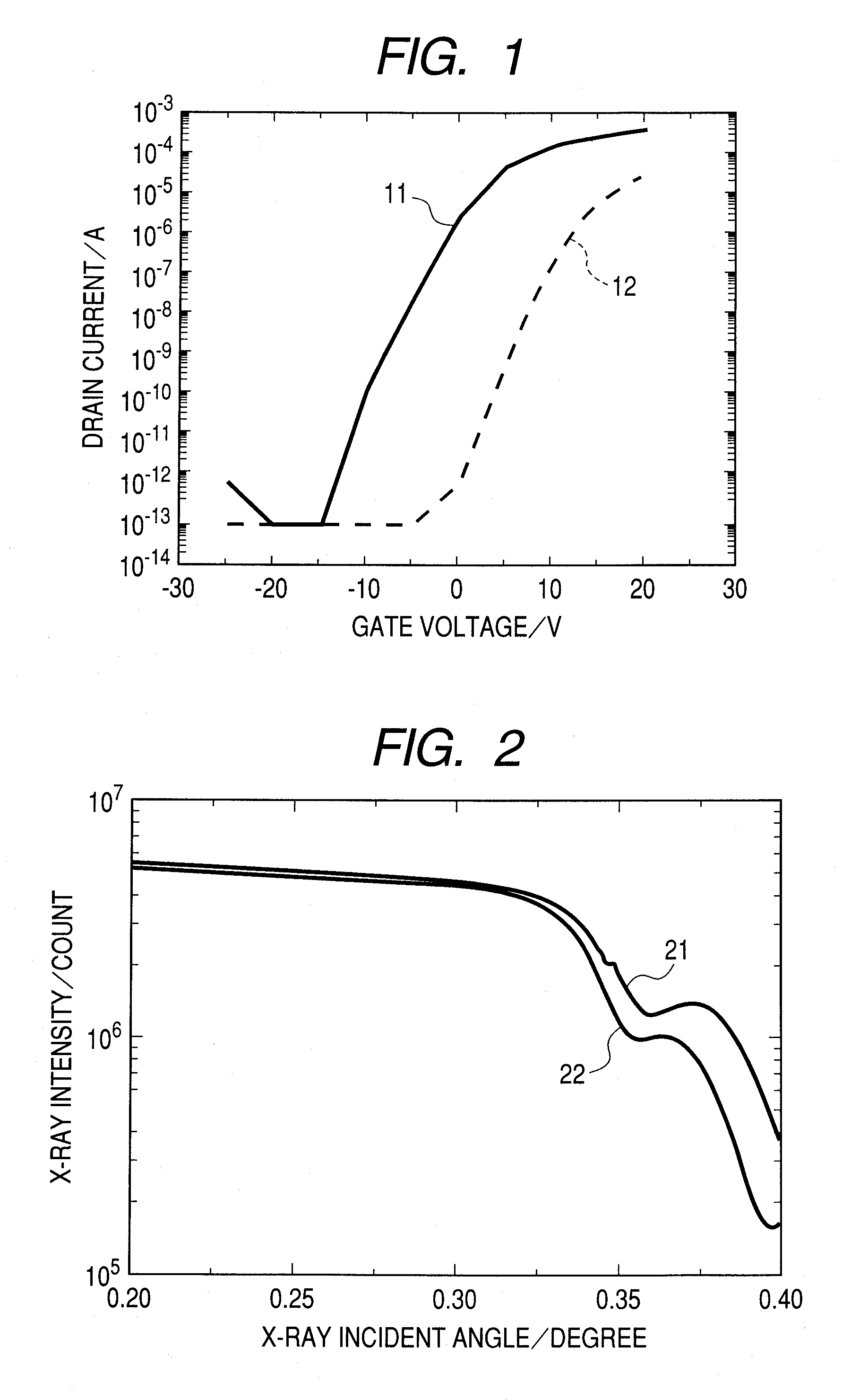
[0047]The obtained film was measured for X-ray reflectivity with an X-ray diffraction apparatus equipped with a Cu—Kα X-ray source and an X-ray mirror. FIG. 2 shows the measurement result by curve 21. Therefrom the film density was estimated at 6.12 g / cm3, 96.2% of the above-estimated theoretical density.

[0048]Separately, another amorphous oxide se...

example 2

Production of TFT Element

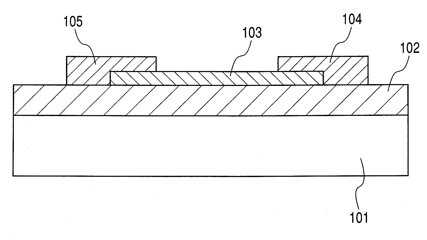
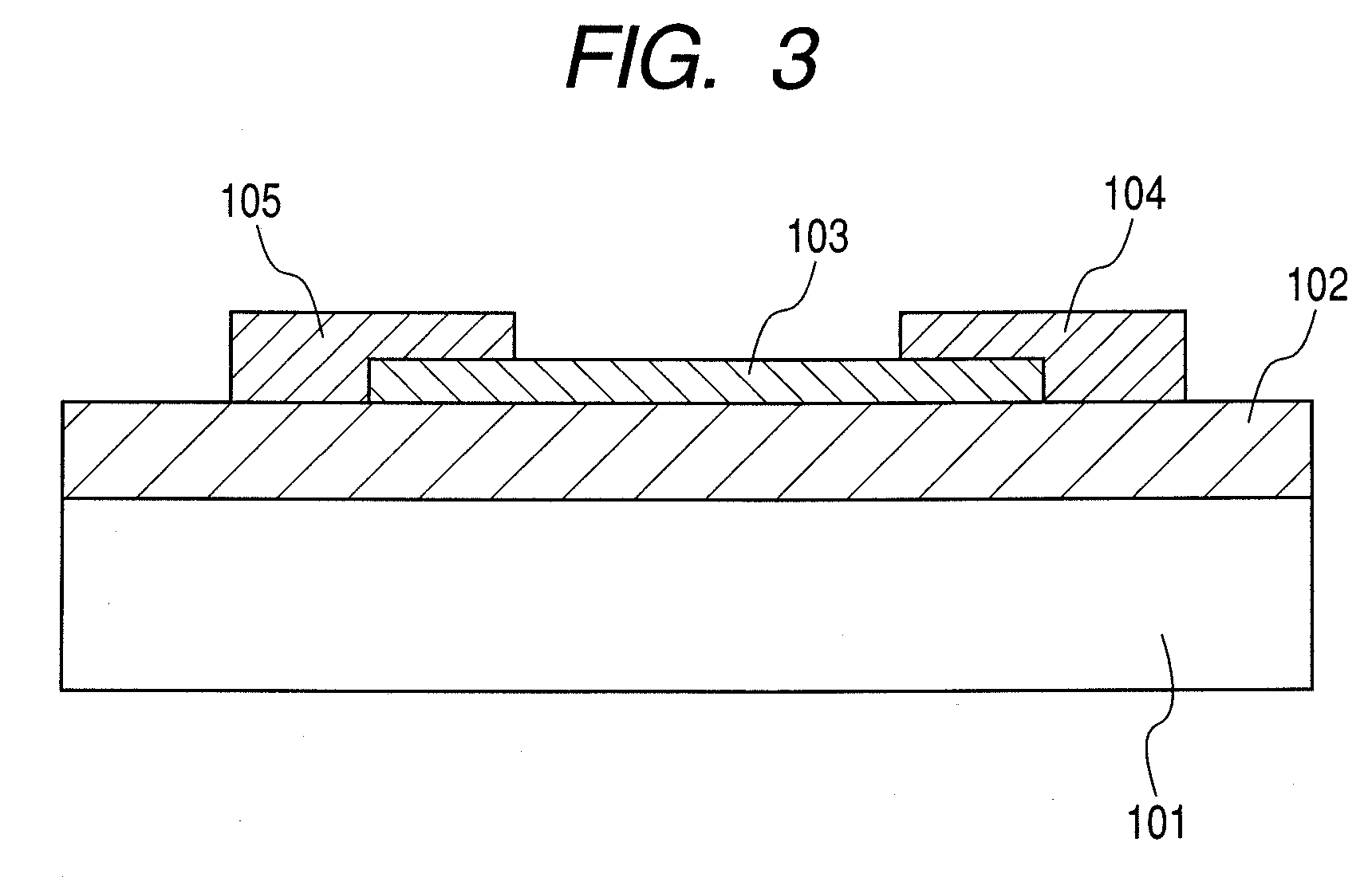
[0057]A bottom-gate type of TFT element illustrated in FIG. 3 was produced as a semiconductor device employing an amorphous oxide semiconductor film.

[0058]Firstly, n-type Si substrate 101 having thereon thermally oxidized SiO2 film 102 of 100 nm thick was prepared. On the SiO2 film, amorphous oxide semiconductor film 103 containing In, Ga, and Zn at a composition ratio of InxGayZnz was formed in a thickness of 40 nm at the substrate temperature of 200° C. by rf-sputtering with an InGaO3(ZnO) target. The obtained film had a density of 96.2% of the theoretical density.

[0059]The obtained amorphous oxide semiconductor film containing In, Ga, and Zn at a composition ratio of InxGayZnz was etched in a necessary size, and then source electrode 104 and drain electrode 105 were formed by photolithography and a lift-off method. The material of the electrodes was a multilayer of Au (150 nm) / Ti (5 nm), and film formation was conducted by electron-beam vapor deposition....


PUM


Abstract

An amorphous oxide semiconductor contains at least one element selected from In, Ga, and Zn at an atomic ratio of InxGayZnz, wherein the density M of the amorphous oxide semiconductor is represented by the relational expression (1) below:
M≧0.94×(7.121x+5.941y+5.675z)/(x+y+z)   (1)
where 0≦x≦1, 0≦y≦1, 0≦z≦1, and x+y+z≠0.

Description

TECHNICAL FIELD[0001]The present invention relates to an amorphous oxide semiconductor, a semiconductor device, and a thin film transistor. In particular, the present invention relates to an amorphous oxide semiconductor containing at least one element selected from In, Ga, and Zn; and a semiconductor device and a thin-film transistor employing the amorphous oxide semiconductor.BACKGROUND ART[0002]Thin-film oxide semiconductors are being studied for use as a channel layer of a transistor. In particular, ZnO oxide-semiconductors are being studied actively for use as a channel of a thin-film transistor (TFT).[0003]However, the thin ZnO film as a semiconductor film, when formed at room temperature, will become polycrystalline and will have several to tens of nanometers of roughness at a semiconductor-insulator interface, a semiconductor-semiconductor interface, or a semiconductor-metal interface: the interface is highly important in the semiconductor device.[0004]Further, in the polycr...

Claims


Application Information

Patent Timeline
IPC IPC(8): H01L29/24H01L29/786
CPCH01L29/247H01L29/66969H01L29/78693H01L29/26H01L29/66742
Inventor YABUTA, HISATOENDO, AYANORIKAJI, NOBUYUKIHAYASHI, RYO
Owner CANON KK
Why Eureka
Try Eureka