

Optical drive device and amplification rate determining method
- Summary
- Abstract
- Description
- Claims
- Application Information
AI Technical Summary
Benefits of technology
Problems solved by technology
Method used
Image

Examples
first embodiment
[0170]A first embodiment of the present invention is explained below in detail with reference to the accompanying drawings.
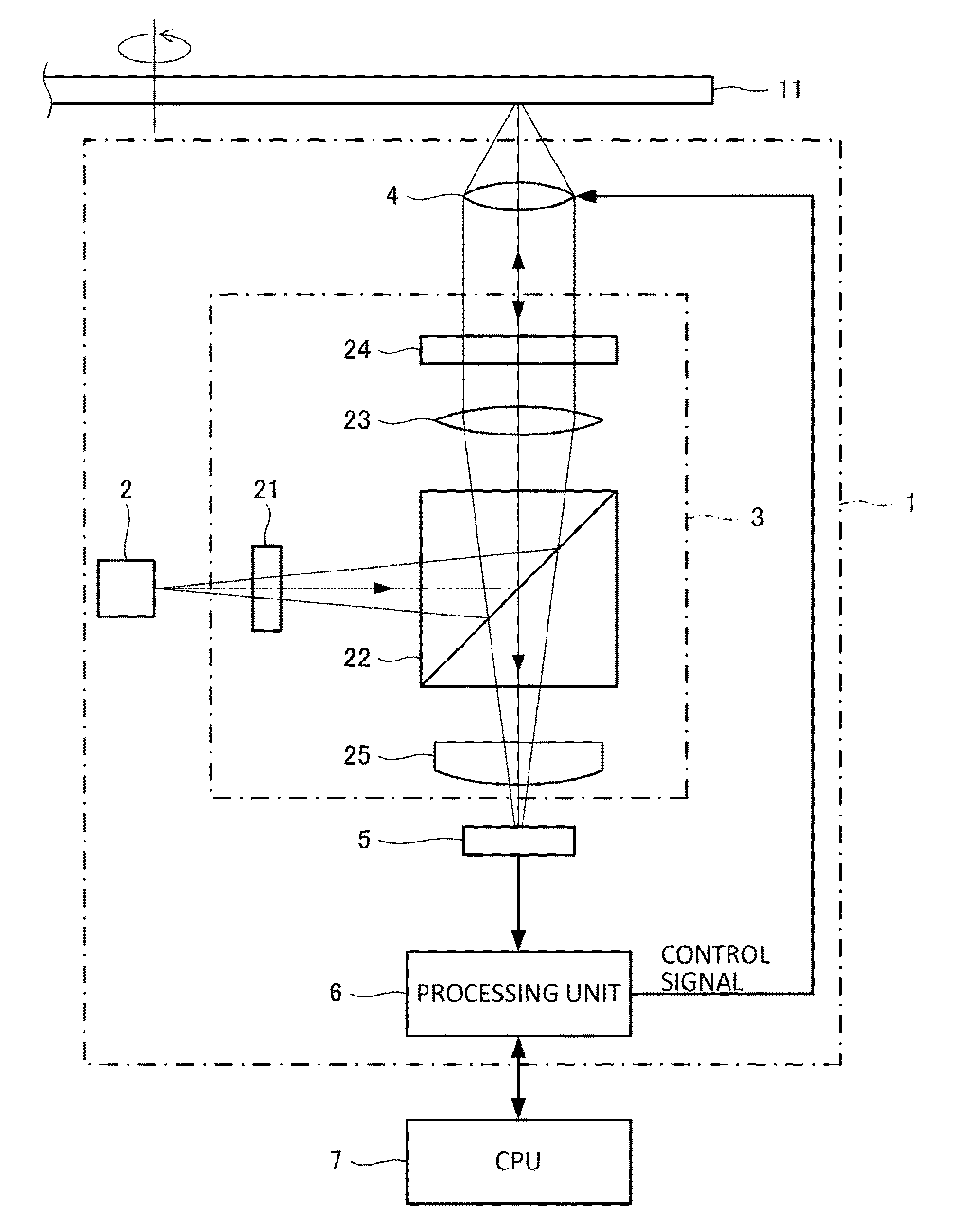
[0171]FIG. 1 is a schematic diagram of an optical drive device 1 according to the first embodiment.
[0172]The optical drive device 1 performs reproduction and recording of the optical disk 11. Various optical recording mediums such as a CD, a DVD, and a BD can be used for the optical disk 11. In the embodiment, particularly a disc-shaped optical disk having a multilayered recording surface using a multilayer film is used.
[0173]As shown in FIG. 1, the optical drive device 1 includes a laser light source 2, an optical system 3, an objective lens 4, an optical detector 5, and a processing unit 6. The laser light source 2, the optical system 3, the objective lens 4, and the optical detector 5 among these units constitute an optical pickup.
[0174]The optical system 3 includes a diffraction grating 21, a beam splitter 22, a collimator lens 23, a quarter-wave plate 24, a...
second embodiment
[0283]A second embodiment of the present invention is explained in detail next with reference to the accompanying drawings.
[0284]Configurations of the optical, drive device 1 and the optical disk 11 according to the second embodiment are similar to the configurations of the optical drive device 1 and the optical disk 11 according to the first embodiment explained with reference to FIG. 1 to FIGS. 7A and 7B, except the following.
[0285]A detailed configuration of the optical detector 5 and a detailed process of the processing unit 6 included in the optical drive device 1 according to the second embodiment are explained below.
[0286]FIG. 20 is a plan view of the optical detector 5 according to the second, embodiment, and shows light receiving surfaces and light receiving areas. FIG. 20 also shows spots of signal light. As shown in FIG. 20, the optical, detector 5 has nine light receiving surfaces including a main-beam receiving surface S1a, sub-beam receiving surfaces S2a and S3a, and s...
second embodiment (
B)
[0421]FIG. 44 shows now to use division lines of the optical detector 5 according to the second embodiment (B). As shown in FIG. 44, in the optical detector 5 according to the second embodiment (B), the main-beam receiving surface S1a is divided into eight areas including divided areas A1, A2, B1, B2, C1, C2, D1, and D2 by the straight lines P1MB, P2MB, P3MB, and Q1MB. These divided areas are arranged, in the order of the divided areas D1, D2, C2, C1, B1, B2, and A2, in a clockwise direction from the divided area A1 positioned at an upper left side of the drawing of the main-beam receiving surface S1a. Hereinafter, the divided areas A1 and D1 are collectively called “light receiving area S1A”, and the divided areas B1 and C1 are collectively called “light receiving area S1B”.
[0422]Similarly, the sub-beam receiving surface S2a is divided, into eight areas including divided areas E1, E2, F1, F2, G1, G2, H1, and H2 by the straight lines P1SB1, P2SB1, P3SB1, and Q1SB1. These divided a...
PUM
 Abstract
Description
Claims
Application Information