Method for manufacturing group iii nitride compound semiconductor light-emitting device, group iii nitride compound semiconductor light-emitting device, and lamp
- Summary
- Abstract
- Description
- Claims
- Application Information
AI Technical Summary
Benefits of technology
Problems solved by technology
Method used
Image
Examples
Example
Examples
[0169]Next is a more detailed description of the method for manufacturing a Group III nitride semiconductor compound light-emitting device of the present invention, with reference to Examples. It should be noted that the present invention is not to be limited to these examples.
Example
Example 1
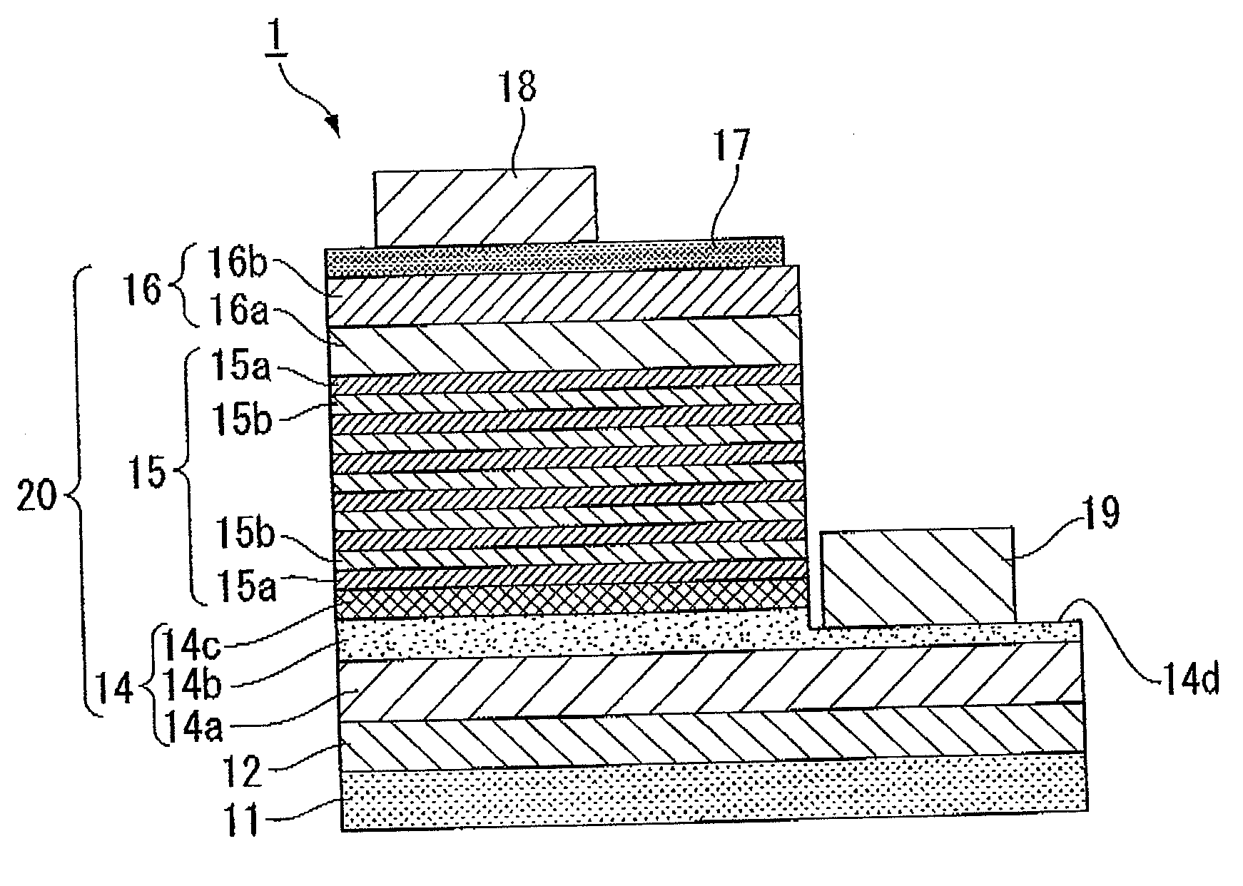
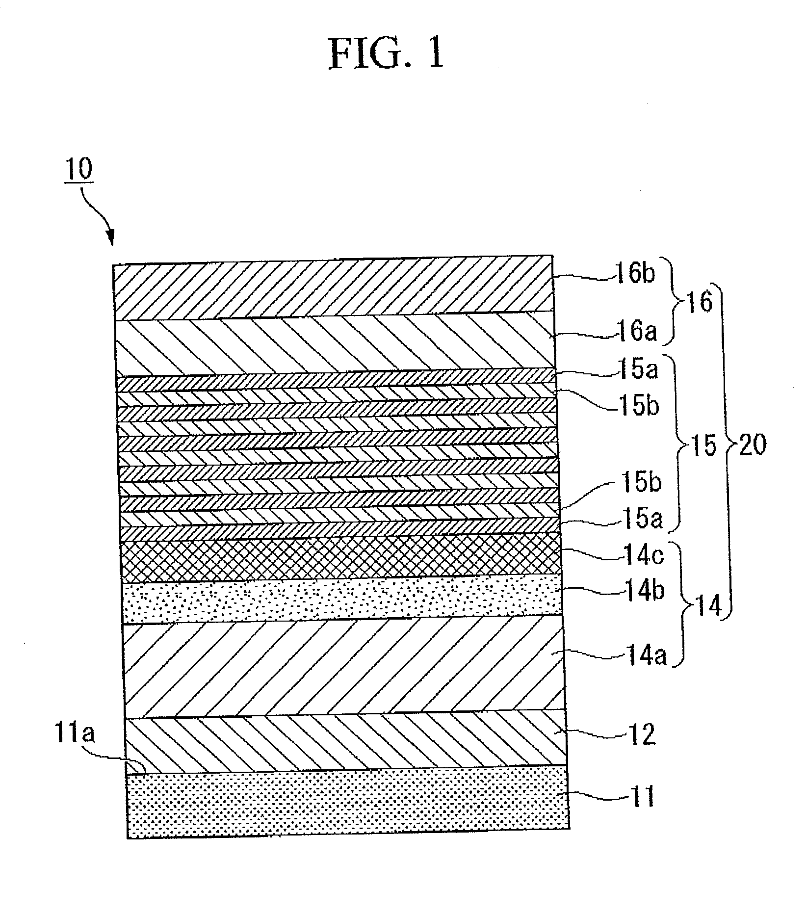
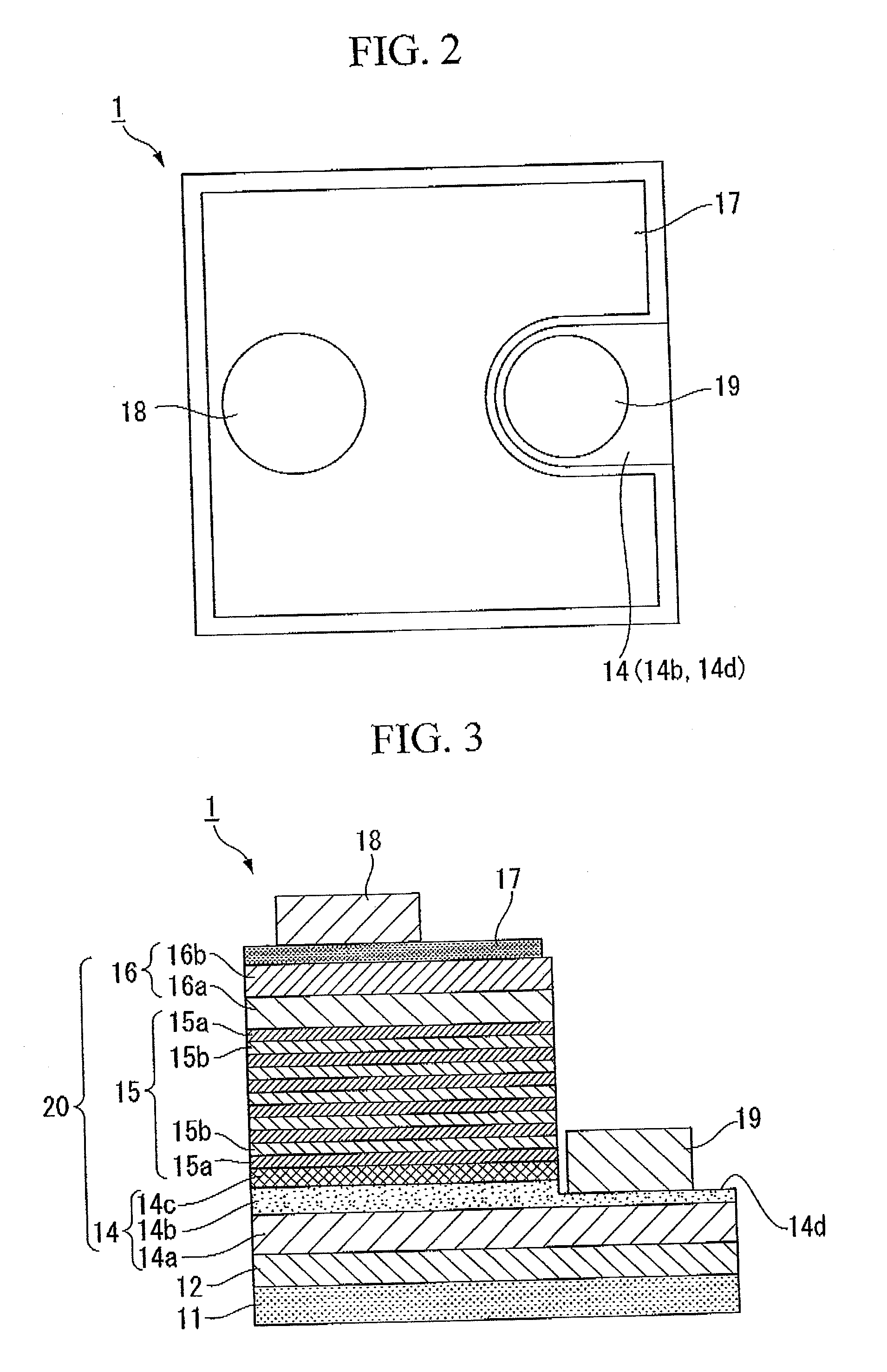
[0170]FIG. 1 illustrates the cross-sectional schematic diagram of the laminated semiconductor of the Group III nitride compound semiconductor light-emitting device produced in the present example.
[0171]In the present example, the aggregate of columnar crystals made of AlN was formed on the c plane of the substrate 11 made of sapphire as the buffer layer 12 using an RF sputtering method. The ground layer 14a and the n-type contact layer 14b were formed thereon as the n-type semiconductor layer 14 using an RF sputtering method that used Ga in a liquid state as a target. On the n-type contact layer 14b, the n-type clad layer 14c was formed using a MOCVD method. Then, the light-emitting layer 15 was formed thereon using a MOCVD method. On the light-emitting layer 15, the p-type clad layer 16a, and the p-type contact layer 16b were formed as the p-type semiconductor layer 16 using an RF sputtering method this order
[0172]At first, the substrate 11 made of sapphire, the one side ...
Example
Comparative Example 1
[0191]In Comparative Example 1, the wafer (laminated semiconductor) was produced in the same manner as Example 1 except that the temperature of cooling water that flows into the ground plate for the sputtering target (target stage 43) was adjusted to −20° C. to thereby cooling the target, and the applied power was adjusted to 0.01 W / cm2 so as not to liquefy the target. Then, the wafer was removed from the reaction apparatus, and it was confirmed that the surface of the wafer was a mirror-like plane.
[0192]In the wafer produced in the above way, the transparent positive electrode was formed, and the positive boding pad and the negative electrode were formed. Then, the backside of the substrate 11 was grinded and polished to make a mirror-like plane, and the wafer was cut into a 350-μm-square chip. The chip was disposed on a lead frame so that the respective electrodes faced upward, and was connected to the lead frame by gold wires. Then, the light-emitting device...
PUM
Property | Measurement | Unit |
---|---|---|
Fraction | aaaaa | aaaaa |
Thickness | aaaaa | aaaaa |
Width | aaaaa | aaaaa |
Abstract
Description
Claims
Application Information
- R&D Engineer
- R&D Manager
- IP Professional
- Industry Leading Data Capabilities
- Powerful AI technology
- Patent DNA Extraction
Browse by: Latest US Patents, China's latest patents, Technical Efficacy Thesaurus, Application Domain, Technology Topic.
© 2024 PatSnap. All rights reserved.Legal|Privacy policy|Modern Slavery Act Transparency Statement|Sitemap