Integrated circuit and a method of making an integrated circuit to provide a gate contact over a diffusion region

a technology of integrated circuits and diffusion regions, applied in the field of integrated circuits, can solve the problems of increasing the difficulty of forming patterns on integrated circuits during manufacture, the difficulty of making the required connections and circuits, and the accuracy and reliability with which such shapes can be produced, so as to reduce the number of process steps, increase the density of sites, and high packing density

Active Publication Date: 2010-03-11
ARM LTD
View PDF8 Cites 10 Cited by
  • Summary
  • Abstract
  • Description
  • Claims
  • Application Information

AI Technical Summary

Benefits of technology

[0026]In another embodiment it may be possible to etch the electrode openings and the gate openings at the same time whilst maintaining a maximum possible etch depth below that at which a short circuit of the gate electrode could arise providing the depths of the openings needed are all sufficiently close together.
[0027]In another technique the substrate and the gate electrode at an early processing stage may be covered with an etch stop layer and then the etch stop layer may be removed from the upper surface of the gate electrode. This prevents etching of the gate opening from reaching the diffusion region.
[0028]A first metal connection layer can be deposited over the at least one electrode connection conductor and the gate connection conductor so as to connect the transistor to other portions of the integrated circuit. This first metal connection layer may be formed as a dual damascene layer with the at least one electrode connection conductor and the gate connection conductor as a single process. Such dual damascene layers help relax alignment constraints and reduce the number of process steps.
[0029]The first metal layer may be formed of rectilinear conductors based substantially perpendicular to the major axis of the local interconnect conductors and gate electrodes. This is useful...

Problems solved by technology

As these device geometries become smaller, it is becoming increasingly difficult to form the patterns on the integrated circuit during manufacture necessary to create the desired circuit elements.
In particular, if it is desired to produce lithographic shapes (patterns) including non-rectilinear shapes, then the accuracy and reliability with which such shapes can be produced is a sig...

Method used


Image

  • Integrated circuit and a method of making an integrated circuit to provide a gate contact over a diffusion region
  • Integrated circuit and a method of making an integrated circuit to provide a gate contact over a diffusion region
  • Integrated circuit and a method of making an integrated circuit to provide a gate contact over a diffusion region

Examples


Embodiment Construction

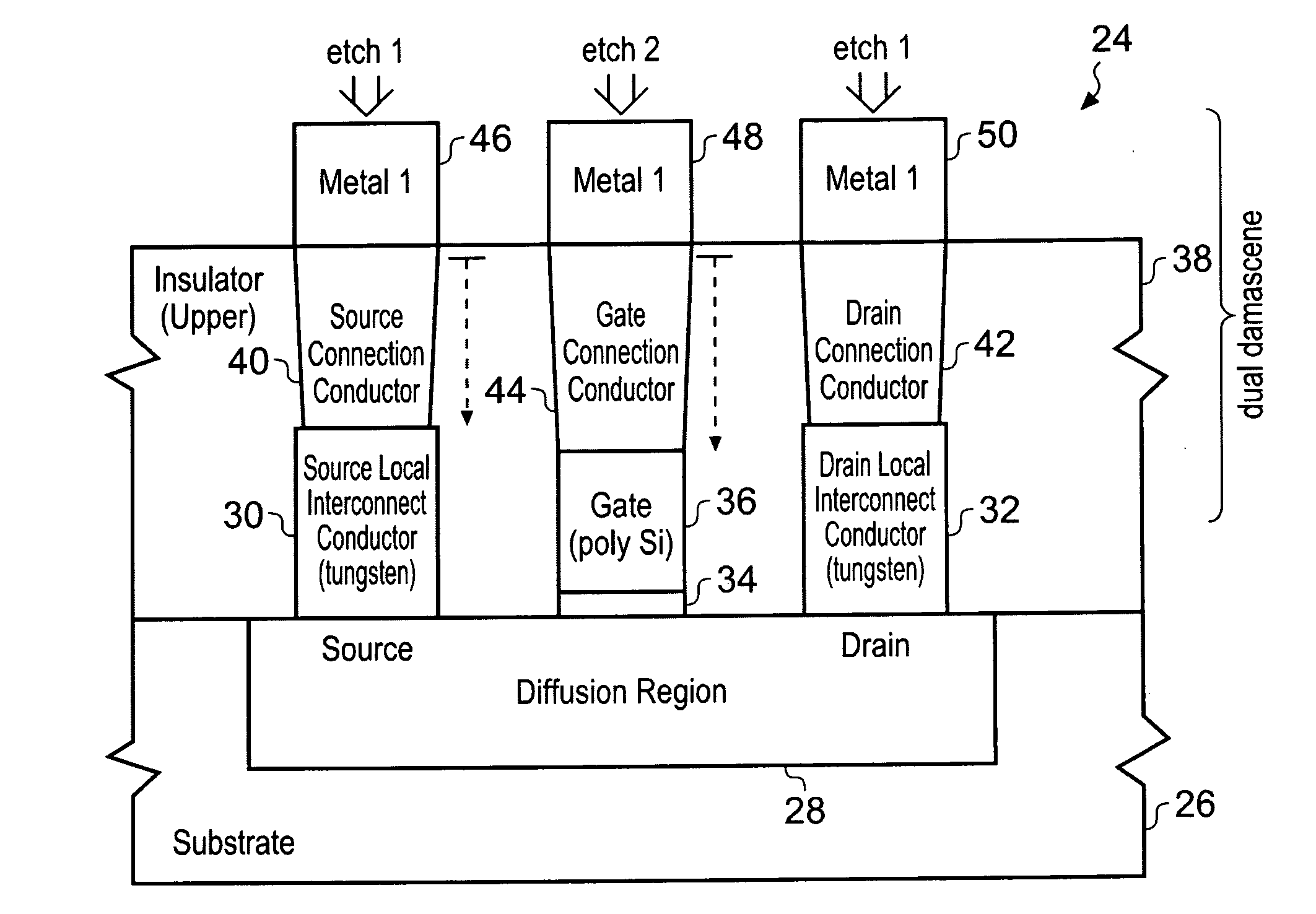
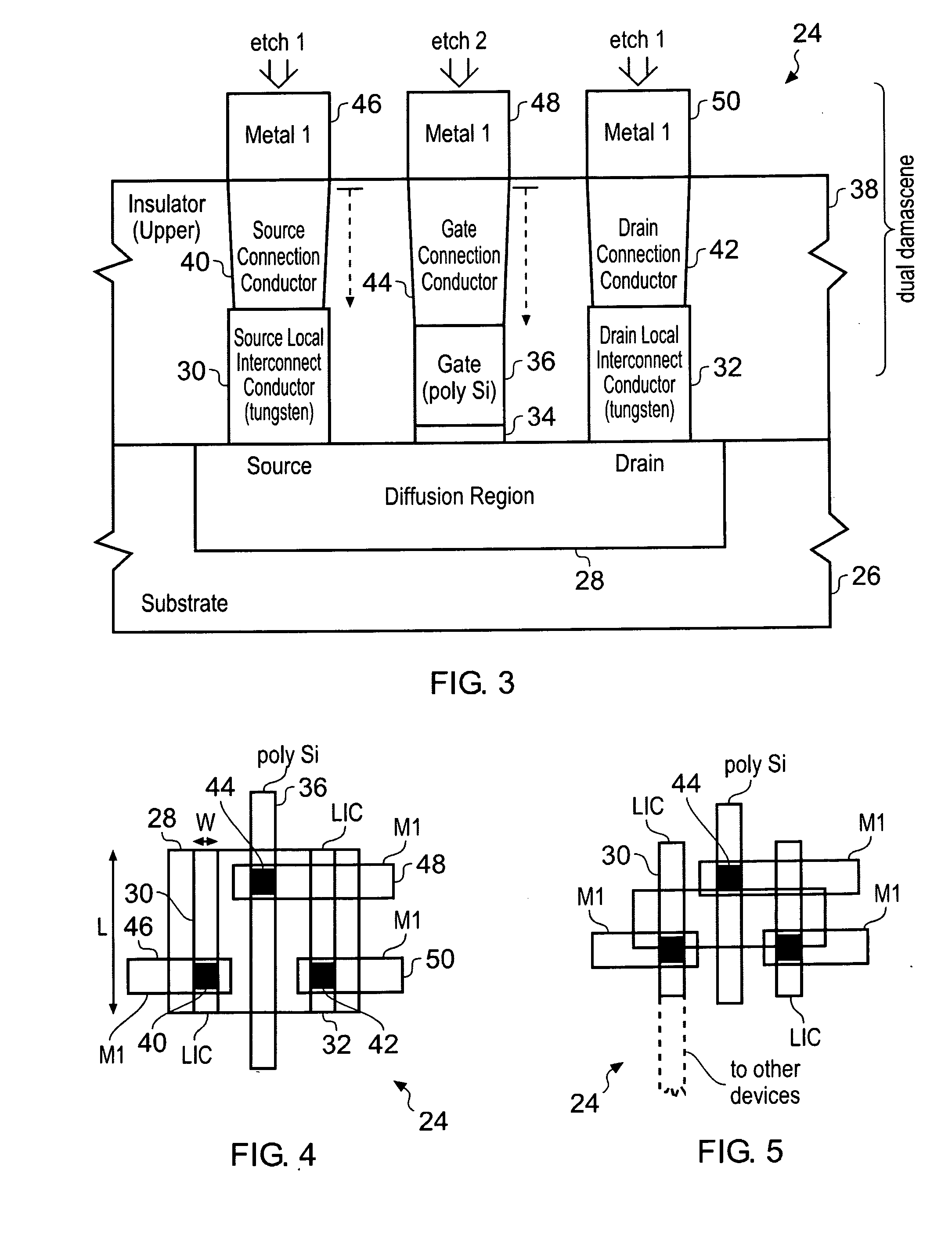
[0062]FIG. 3 is a side projection view of a transistor 24. A substrate 26 is provided with a diffusion region 28. The diffusion region 28 may, for example, be formed by dopant implantation using techniques familiar to those in this technical field. Over the diffusion region 28 there are then formed a source local interconnect conductor 30 and a drain local interconnect conductor 32. Both of these may be formed of tungsten and have a pure rectilinear shape extending out of the plane of FIG. 3. The formation of the source local interconnect conductor 30 and the drain local interconnect conductor 32 may use conventional lithographic techniques. These lithographic techniques are aided by the pure rectilinear form of the source local interconnect conductor 30 and the drain local interconnect conductor 32. These pure rectilinear forms are such that the length L of the source local interconnect conductor 30 and the drain local interconnect conductor 32 is at least three times greater than ...


PUM


Abstract

A method of forming an integrated circuit 68 provides over a diffusion region 28 on a substrate 26 a gate electrode 36. A source electrode is provided by a source local interconnect conductor 30 and a drain electrode is provided by a drain local interconnect conductor 32. An insulator layer 38 is formed over these electrodes and respective electrode openings are formed through the insulator layer 38 so as to provide electrical connection to a Metal1 layer 46, 48, 50. The etching process for the electrode openings is controlled such that the maximum etching depth is insufficient to penetrate through the insulating layer 38 and accordingly short circuit a gate insulator layer 34 provided between the diffusion region 28 and the gate electrode 36. Thus, the gate opening may be positioned over the diffusion region 28. Double patterning followed by separate etching steps for the gate opening and the source/drain opening may be used to control the gate opening depth and permit the gate contact to be position overlying the diffusion region.

Description

BACKGROUND OF THE INVENTION[0001]1. Field of the Invention[0002]This invention relates to the field of integrated circuits. More particularly, this invention relates to a method of making integrated circuits and integrated circuits utilising local interconnect conductors.[0003]2. Description of the Prior Art[0004]It is known to make and provide integrated circuits formed from processes involving multiple stages of lithography, deposition, etching, implantation etc. Advances in these processes have permitted device geometries to reduce thereby increasing the circuit density achievable and reducing cost. Recent production geometries have used devices with feature sizes of 45 nm. Projected future devices are expected to have sizes of 32 nm followed by 22 nm. As these device geometries become smaller, it is becoming increasingly difficult to form the patterns on the integrated circuit during manufacture necessary to create the desired circuit elements. In particular, if it is desired to...

Claims


Application Information

Patent Timeline
IPC IPC(8): H01L21/768H01L23/532H01L23/522
CPCH01L21/76816H01L29/66545H01L27/0207H01L21/76895
Inventor YERIC, GREGORY MUNSONFREDERICK, MARLIN WAYNE
Owner ARM LTD
Why Eureka
Try Eureka