SINGLE PHOTON SOURCE WITH AllnN CURRENT INJECTION LAYER

a single photon source and injection layer technology, applied in semiconductor devices, lasers, semiconductor lasers, etc., can solve the problems of poor manufacturing yield, limiting working temperature, cumbersome and expensive, etc., and achieve the effect of high efficiency and easy reachability

Inactive Publication Date: 2010-03-18
SHARP KK
View PDF5 Cites 7 Cited by
  • Summary
  • Abstract
  • Description
  • Claims
  • Application Information

AI Technical Summary

Benefits of technology

[0010]So it is an object of the present invention to address the above problems, by providing a single photon source with high efficiency working at room temperature or temperatures easily reachable with thermo-electric cooling.

Problems solved by technology

But the first three sources require optical excitation of carriers using an external laser source, which is cumbersome and expensive.
However, the device used self-assembled InAs quantum dots, thus limiting the working temperature to 10-100° K. Moreover, an annulus of insulating aluminium oxide was used to limit the current injection to a single quantum dot.
But uniformity control of the oxidation process is known as an issue which can result to current apertures with different dimensions over the wafer, leading to poor manufacturing yield.
However, the main obstacle for commonly used epitaxially grown III-V quantum dots as single photon devices, such as InAs quantum dots, is the requirement of liquid helium cryogenic temperatures.
But the quantum efficiency and multi-phonon reduction efficiency at high temperatures were low.
Though there have been many demonstrations of single photon sources using quantum dots with electrical injection of the carriers, they all required liquid-helium cryogenic temperatures, which is the main obstacle for industrial application.

Method used


Image

  • SINGLE PHOTON SOURCE WITH AllnN CURRENT INJECTION LAYER
  • SINGLE PHOTON SOURCE WITH AllnN CURRENT INJECTION LAYER

Examples


Embodiment Construction

[0037]The preferred embodiments of the invention will be described with reference of the drawings.

[0038]A device of the present invention may be grown by any suitable means and on any suitable substrate, which include but is not limited to any orientation of: sapphire, GaN or SiC.

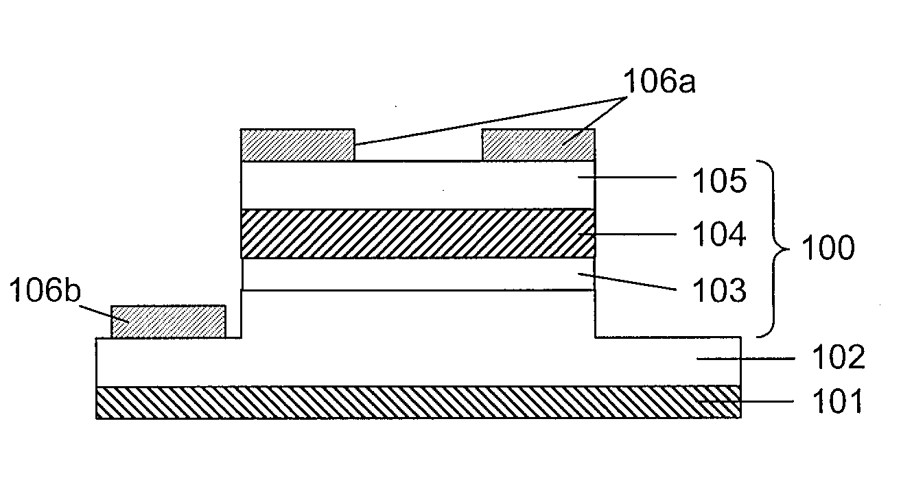
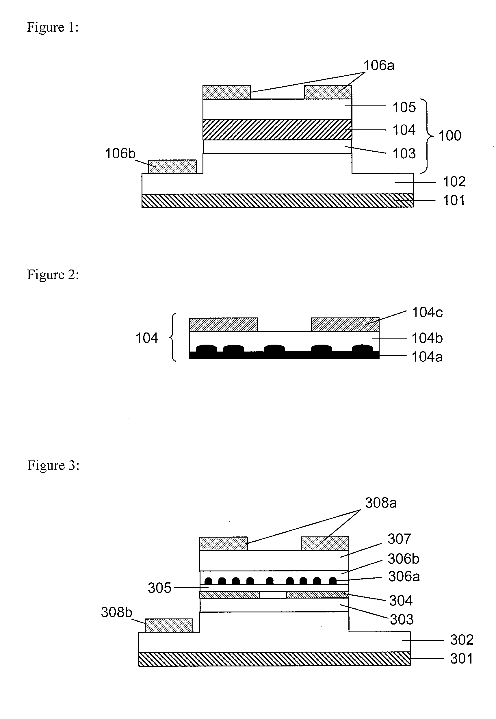
[0039]The first embodiment of the present invention is described with reference to FIG. 1. According to the first embodiment of this invention, FIG. 1 shows a schematic of a single photon emitting device fabricated in the (Al,In,Ga)N material system. The single photon emitting device of FIG. 1 may contain a sapphire substrate 101. An n-type buffer layer 102 made in the (Al,In,Ga)N material system, and preferentially in the (Al,Ga)N material system may be disposed on top of the substrate 101. A non-intentionally doped (Al,Ga)N layer 103 may be disposed on top of the buffer layer 102 to improve injection efficiency of the carriers. The active region 104 is then disposed on top of the layer 103. A p-type (Al,G...


PUM


Abstract

A photon source includes a substrate, an active region formed above the substrate, and a pair of electrodes configured to provide an injection current which passes through the active region. The active region includes a quantum dot layer including one or more AlyGaxIn1-x-yN quantum dots, where 0≦x≦1 and 0≦y≦<1, and an AlInN current confinement layer adjacent the quantum dot layer. The current confinement layer has an aperture which defines a low resistance path for the injection current to flow through the active region between the pair of electrodes. The quantum dot layer includes less than 50 quantum dots within the aperture as projected onto the quantum dot layer.

Description

TECHNICAL FIELD [0001]The present invention relates to the field of light emitting devices which are capable of emitting a predetermined number of photons at predetermined times, and more specifically which are capable of emitting a single photon on demand.BACKGROUND OF THE INVENTION [0002]Quantum information in the form of quantum communications and quantum computing is currently an exceedingly active field. A single source that efficiently produces photons with antibunching characteristics or an entangled-pair of photons is one such pivotal hardware element for quantum information technology. Using a single photon source, secure quantum communication will prevent any potential eavesdropper from intercepting a message without the receiver noticing. Indeed, it works on the fact that measurement of a quantum state causes a disturbance which can be detected by the sender and the intended recipient of the bits.[0003]There are four main possible sources for single photons; these are a s...

Claims


Application Information

Patent Timeline
Patent Type & Authority Applications(United States)
IPC IPC(8): H01L33/00
CPCB82Y20/00H01S5/34333H01S5/3412H01S5/221
Inventor SENES, MATHIEU XAVIERSMITH, KATHERINE LOUISEBROADLEY, VICTORIAHOOPER, STEWART EDWARD
Owner SHARP KK
Why Eureka
Try Eureka