Method for manufacturing thin film transistor using oxide semiconductor and display apparatus

a technology of oxide semiconductor and display apparatus, which is applied in the direction of transistors, electrical devices, semiconductor devices, etc., can solve the problems of reducing the electric resistance of destroying the exposed oxide semiconductor layer, and achieve excellent transistor characteristics

Active Publication Date: 2010-03-18
CANON KK
View PDF19 Cites 138 Cited by
  • Summary
  • Abstract
  • Description
  • Claims
  • Application Information

AI Technical Summary

Benefits of technology

[0015]Thus, in a thin film transistor using an oxide semiconductor according to the present invention, the electric resistance of a contact region of the oxide semiconductor layer to be held in contact with an electrode can be lowered and forming an ohmic contact with a source electrode or a drain electrode. Therefore, the present invention can provide a thin film transistor showing excellent transistor characteristics in terms of ohmic contact.

Problems solved by technology

As a result of the above step, the exposed oxide semiconductor layer is damaged and its electric resistance is lowered to form a contact region.

Method used


Image

  • Method for manufacturing thin film transistor using oxide semiconductor and display apparatus
  • Method for manufacturing thin film transistor using oxide semiconductor and display apparatus
  • Method for manufacturing thin film transistor using oxide semiconductor and display apparatus

Examples


example 1

[0086]In this example, reverse staggered (bottom gate) type MISFET devices were prepared. For each device, firstly a gate terminal of Ti5 nm / Au40 nm / Ti5 nm was prepared on a glass substrate by means of photolithography and a lift-off method. Then, an insulating layer of amorphous SiOx was formed to a thickness of 200 nm thereon by sputtering. At this time, an SiO2 target was used as sputtering target and Ar gas was used as sputtering gas. The RF high frequency power and the film forming pressure were 400 W and 0.1 Pa respectively. The substrate temperature was room temperature and the substrate was not intentionally heated. Then, an amorphous oxide semiconductor film to be used as semiconductor layer was formed to a thickness of 20 nm by sputtering at room temperature. At this time, a polycrystalline InGaZnO4 target was employed and an O2 / Ar gas with a mixing ratio of 5 vol % was used as sputtering gas. The RF high frequency power and the film forming pressure were 200 W and 0.1 Pa ...

example 2

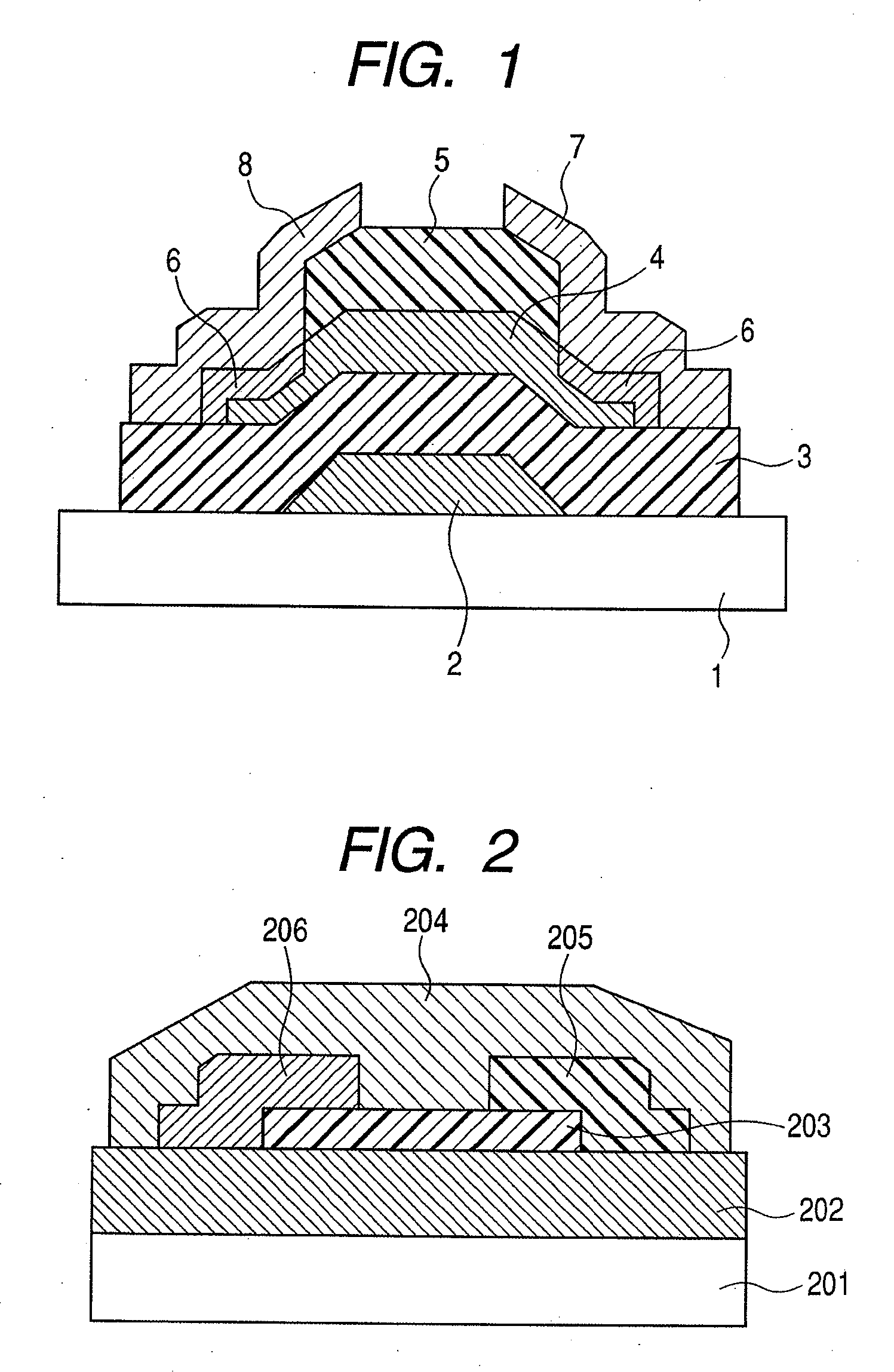
[0088]Reverse staggered (bottom gate) type MISFET devices as shown in FIG. 11 were prepared as in Example 1 except the conditions for forming the second insulating film.

[0089]For each device, an insulating layer of amorphous SiOx was formed to a thickness of 100 nm as the second insulating film by sputtering. An oxidative gas atmosphere containing O2 / Ar mixture gas with a mixing ratio of 10 vol % was used as sputtering gas. A total of nine reverse staggered (bottom gate) type MISFET devices as shown in FIG. 11 were completed in this way.

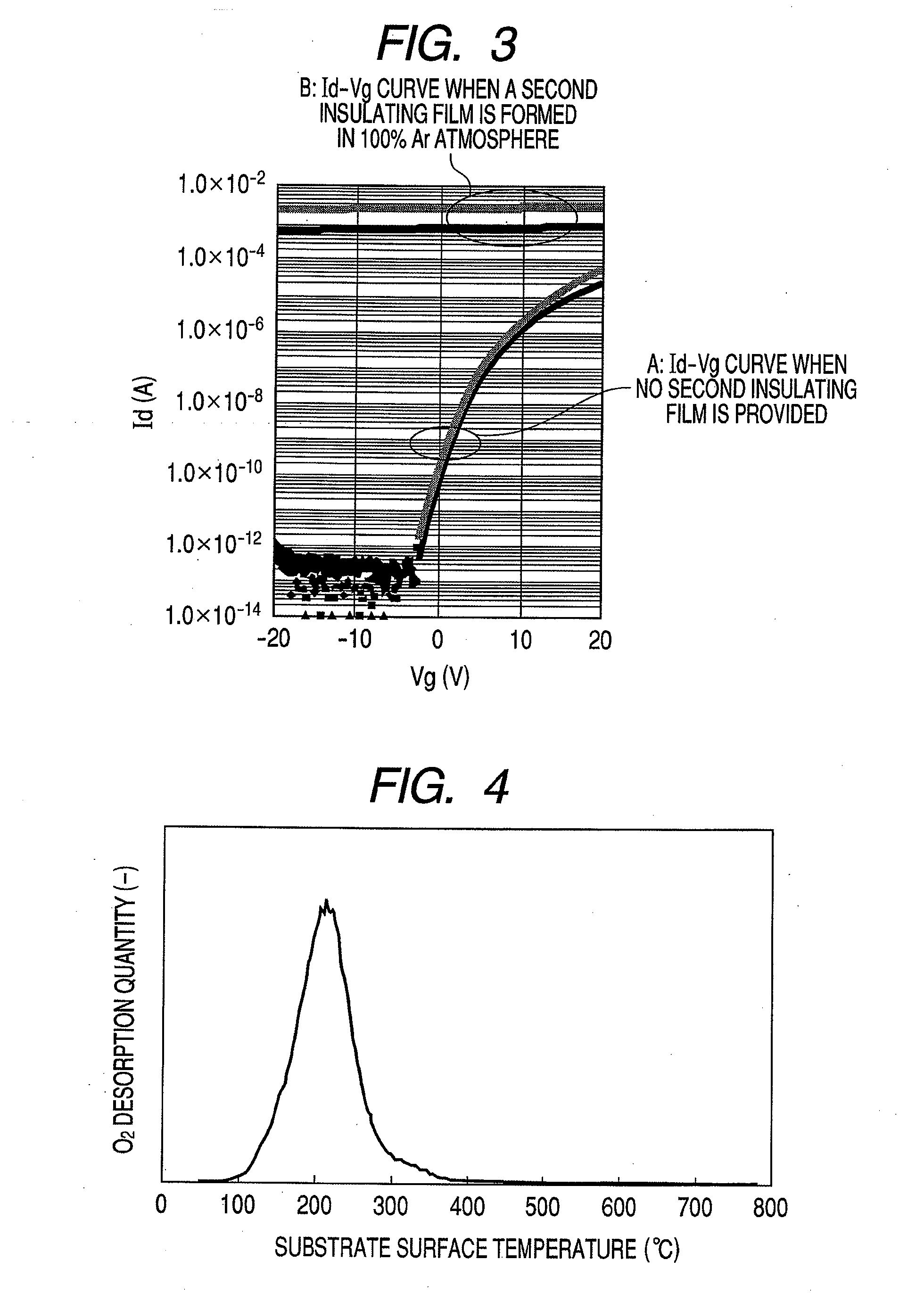
[0090]At the same time, a TEG device for gauging the oxide semiconductor electric conductivity was prepared under the same process conditions and the electric conductivity of the oxide semiconductor layer was observed. FIG. 9 is a graph illustrating the relationship between Von and the electric conductivity of the oxide semiconductor. In FIG. 9, Von denotes the voltage applied to the gate when the drain current (Id) rises with the transfer characteri...

example 3

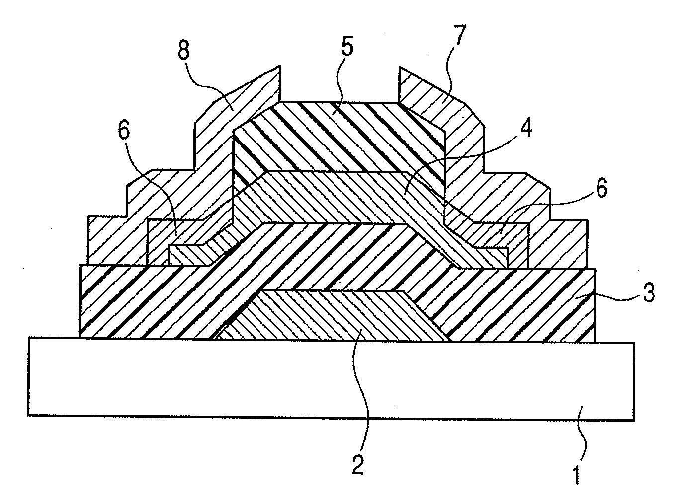
[0095]In this example, a reverse staggered (bottom gate) type MISFET device illustrated in FIG. 1 was prepared.

[0096]Firstly, a gate electrode layer of transparent conductive film IZO was formed to a thickness of 150 nm on a glass substrate by sputtering. The gate electrode was formed by means of photolithography and wet etching using hydrochloric acid. Additionally, an insulating layer of amorphous SiOx was formed to a thickness of 200 nm thereon also by sputtering. At this time, an SiO2 target was used as sputtering target and Ar gas was used as sputtering gas. The RF high frequency power and the film forming pressure were 400 W and 0.1 Pa respectively. The substrate temperature was room temperature and the substrate was not intentionally heated. Then, an amorphous oxide semiconductor film to be used as semiconductor layer was formed to a thickness of 20 nm by sputtering at room temperature. At this time, a polycrystalline InGaZnO4 target was employed and an O2 / Ar gas with a mixin...


PUM


Abstract

A thin film transistor is manufactured by forming a gate electrode on a substrate, forming a first insulating film on the gate electrode, forming an oxide semiconductor layer on the first insulating film with an amorphous oxide, patterning the first insulating film, patterning the oxide semiconductor layer, forming a second insulating film on the oxide semiconductor layer in an oxidative-gas-containing atmosphere, patterning the second insulating film to expose a pair of contact regions, forming an electrode layer on the pair of contact regions, and patterning the electrode layer to for a source electrode and a drain electrode.

Description

TECHNICAL FIELD[0001]This invention relates to a method of manufacturing a thin film transistor using an oxide semiconductor and a display apparatus.BACKGROUND ART[0002]Thin film transistors having a silicon-based semiconductor layer have been and being employed for switching elements of display apparatus that may be active matrix type liquid crystal display devices or organic electroluminescent devices. For instance, a gate electrode is formed on an insulating substrate and subsequently a gate insulating film is formed on the insulating substrate that includes the gate electrode. Thereafter, a semiconductor layer of amorphous silicon is formed thereon. Then, a channel protective film is formed in a center area of the upper surface of the semiconductor layer and an ohmic contact layer of n-type amorphous silicon is formed at the opposite sides of the protective film on the semiconductor channel layer. Subsequently, a source electrode and a drain electrode are arranged on the ohmic c...

Claims


Application Information

Patent Timeline
Patent Type & Authority Applications(United States)
IPC IPC(8): H01L29/786H01L21/34H01L33/00H01L21/336
CPCH01L29/7869H01L27/1225H01L29/45H01L29/78606
Inventor OMURA, HIDEYUKIHAYASHI, RYOKAJI, NOBUYUKIYABUTA, HISATO
Owner CANON KK
Why Eureka
Try Eureka