Porous device for optical and electronic applications and method of fabricating the porous device

a technology of optical and electronic applications and porous devices, applied in the field of porous single crystal structure, can solve the problems of amorphous or polycrystalline materials with poor electronic properties, the difficulty of fabricating 3d photonic crystals with complete or near complete photonic band gaps and the required electronic properties, and the inability to realize ideas, etc., to achieve the effect of improving the efficiency of existing optical and electronic devices, ensuring advantageous electrical properties, and substantial

Active Publication Date: 2010-03-18
THE BOARD OF TRUSTEES OF THE UNIV OF ILLINOIS
View PDF6 Cites 7 Cited by
  • Summary
  • Abstract
  • Description
  • Claims
  • Application Information

AI Technical Summary

Benefits of technology

[0007]The inventors have developed a method of creating porous 3D single-crystal structures with photonic and electronic functionality. These structures have substantial control over light that interacts with them while maintaining advantageous electrical properties (e.g., conductivity and carrier mobility). This unique combination of electrical properties and optical control in a single three-dimensional material structure may allow greatly improved efficiency of existing optical and electronic devices, as well as enabling entirely new devices.

Problems solved by technology

However, these ideas have yet to come to fruition and the optoelectronics research space has been dominated by work on two-dimensional photonic crystals.
The fundamental limiting factor for moving into 3D devices is the difficulty of fabricating 3D photonic crystals with complete or nearly complete photonic band gaps and the required electronic properties (e.g., high mobility and low defect density).
Most fabrication techniques, in particular those which are rapid, flexible in terms of structure, and commercially relevant, result in amorphous or polycrystalline materials with poor electronic properties.
Those which can create single-crystal structures, such as wafer bonding and layer-by-layer assembly, are hindered by slow fabrication times and limitations on the possible photonic crystal structures.
In addition, electrically driven emission has not been demonstrated for single-crystal structures resulting from fabrication techniques.

Method used


Image

  • Porous device for optical and electronic applications and method of fabricating the porous device
  • Porous device for optical and electronic applications and method of fabricating the porous device
  • Porous device for optical and electronic applications and method of fabricating the porous device

Examples


Embodiment Construction

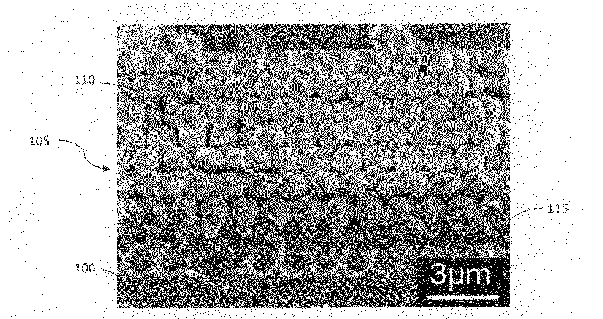
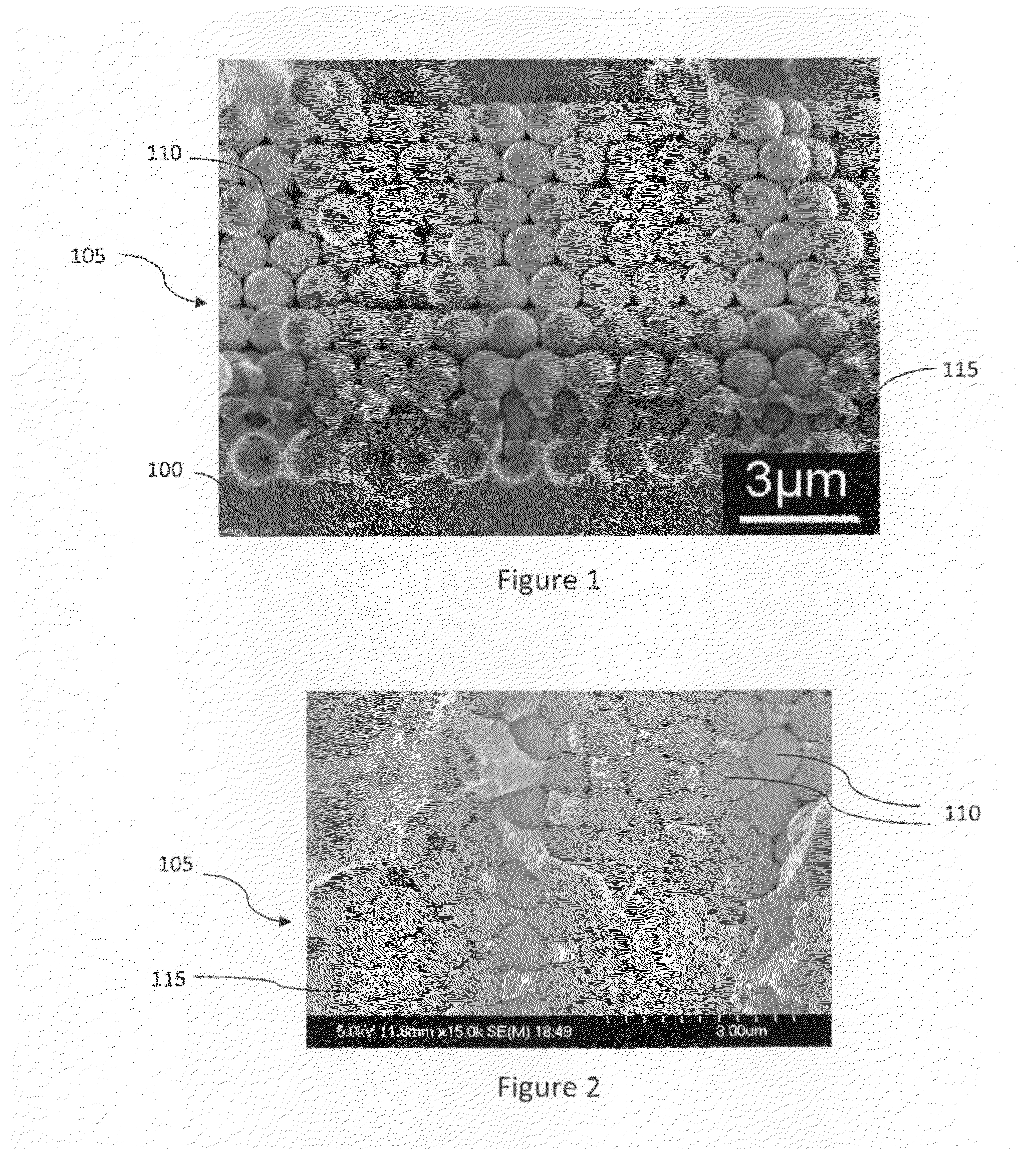
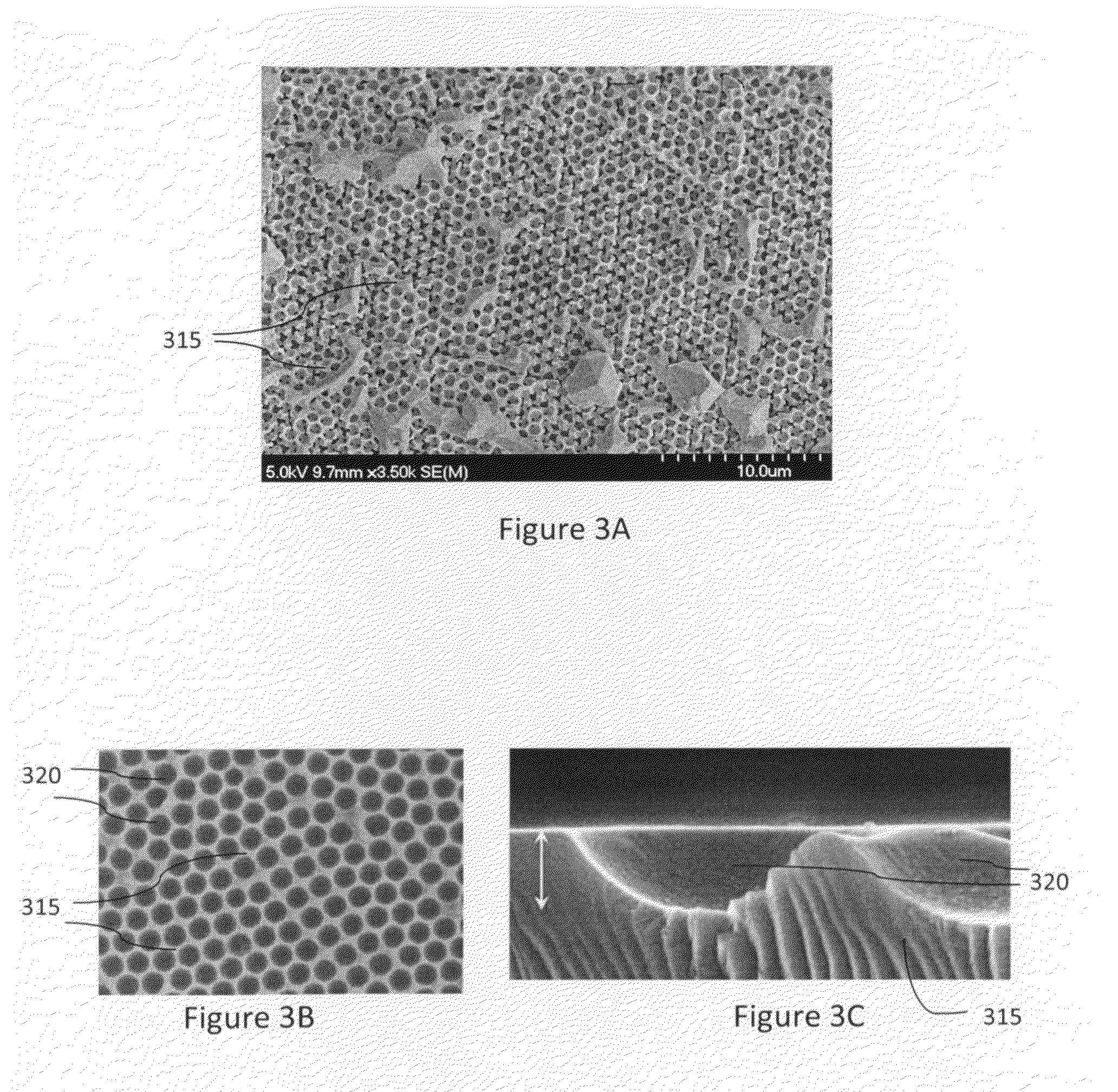
[0023]Described herein is a new approach for fabricating single crystal, three-dimensional (3D) porous structures for photonic and optoelectronic applications based on the selective area epitaxy of materials such as III-V semiconductors. The approach allows epitaxial growth of the single crystal structures through three-dimensional scaffolds or templates to produce high-quality optical and electronic devices.

[0024]The fabrication method involves forming a three-dimensional scaffold on a single crystal substrate. The scaffold typically has characteristic dimensions ranging from tens of nanometers to a few microns. The terms template and scaffold are used interchangeably throughout this disclosure in reference to the framework of interconnected elements employed to direct growth of the 3D single crystal structure on the substrate. The scaffold, which is typically formed of an insulating material, is constructed on the single crystal substrate by colloidal assembly, lithography, or ano...


PUM

PropertyMeasurementUnit
thicknessaaaaaaaaaa
temperatureaaaaaaaaaa

Abstract

A porous device for optical and electronic applications comprises a single crystal substrate and a porous single crystal structure epitaxially disposed on the substrate, where the porous single crystal structure includes a three-dimensional arrangement of pores. The three-dimensional arrangement may also be a periodic arrangement. A method of fabricating such a device includes forming a scaffold comprising interconnected elements on a single crystal substrate, where the interconnected elements are separated by voids. A first material is grown epitaxially on the substrate and into the voids. The scaffold is then removed to obtain a porous single crystal structure epitaxially disposed on the substrate, where the single crystal structure comprises the first material and includes pores defined by the interconnected elements of the scaffold.

Description

RELATED APPLICATION[0001]The present patent document is a continuation-in-part of U.S. patent application Ser. No. 11 / 733,151, which was filed on Apr. 9, 2007, and is hereby incorporated by reference in its entirety.FEDERALLY SPONSORED RESEARCH OR DEVELOPMENT[0002]This material is based upon work supported in part by the U. S. Army Research Laboratory and the U. S. Army Research Office under contract / grant number DAAD19-03-1-0227. The U.S. government may have rights in this invention.TECHNICAL FIELD[0003]This disclosure is related generally to devices for optical and electronic applications and more particularly to porous single crystal structures with photonic and electronic functionality.[0004]BACKGROUND[0005]Since their conception over 20 years ago, three-dimensional (3D) photonic crystals have been touted for their extraordinary potential in the area of optoelectronics. However, these ideas have yet to come to fruition and the optoelectronics research space has been dominated by...

Claims


Application Information

Patent Timeline
Patent Type & Authority Applications(United States)
IPC IPC(8): H01L29/20H01L21/20
CPCH01C7/10Y10T428/249953
Inventor BRAUN, PAUL V.COLEMAN, JAMES J.ELARDE, VICTOR C.NELSON, ERIK C.VERMA, VARUN B.
Owner THE BOARD OF TRUSTEES OF THE UNIV OF ILLINOIS
Why Eureka
Try Eureka